
why use etch back bga substrate design
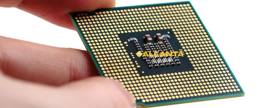
Ball Grid Array (BGA) substrates serve as critical components in modern electronics, facilitating the connection between integrated circuits and printed circuit boards (PCBs). These substrates feature a grid of solder balls underneath the chip, enabling efficient heat dissipation and electrical connectivity. However, to optimize the performance and reliability of BGA substrates, manufacturers employ advanced fabrication techniques such as etch back.
Etch back, a crucial process in semiconductor manufacturing, involves selectively removing material layers to achieve desired electrical and mechanical properties. In the context of BGA substrate design, etch back plays a vital role in fine-tuning the substrate’s dimensions, ensuring precise alignment and robust interconnection. Understanding the significance of etch back in BGA substrate design is essential for engineers and manufacturers striving for excellence in electronic component production.
Understanding Etch Back: Enhancing BGA Substrate Design
Definition of Etch Back in Semiconductor Manufacturing
Etch back, a fundamental process in semiconductor manufacturing, involves selectively removing material layers from a substrate to achieve desired dimensions and properties. In the context of BGA substrate design, etch back enables precise adjustment of substrate thickness and alignment, ensuring optimal electrical and mechanical performance.
Positive Etchback vs. Negative Etchback: Understanding the Variants
Positive etchback involves removing material from the surface of the substrate, effectively reducing its thickness. Conversely, negative etchback entails removing material from the substrate’s edges or inner layers, altering its overall shape or dimensions. Both variants are essential for achieving specific design requirements and optimizing the substrate’s functionality in BGA applications.
Importance of Etchback in Optimizing Substrate Performance
Etchback plays a crucial role in enhancing the performance and reliability of BGA substrates. By precisely controlling substrate dimensions and alignment, etchback ensures uniform solder ball deposition and robust interconnection between the chip and PCB. This optimization is paramount in high-density electronic assemblies where space constraints demand utmost precision. Overall, the strategic implementation of etchback significantly contributes to the success of BGA substrate designs, meeting the rigorous demands of modern electronics.
Exploring Etchback in PCB Design: Enhancing BGA Substrate Functionality
The Need for Etching in PCB Fabrication
In the realm of PCB (Printed Circuit Board) fabrication, etching is indispensable for achieving precise circuit patterns and interconnections. As the complexity of electronic devices increases, the demand for compact and high-performance PCBs intensifies. Etching enables the removal of unwanted copper from the substrate, delineating intricate pathways for electrical signals to traverse. This precision is essential for ensuring optimal functionality and performance in modern electronic assemblies.
Etchback’s Role in Enhancing PCB Functionality and Reliability
Etchback plays a pivotal role in optimizing the functionality and reliability of PCBs, particularly in the context of BGA (Ball Grid Array) substrate design. By fine-tuning the dimensions and alignment of the substrate, etchback facilitates the deposition of solder balls with utmost precision. This meticulous control ensures secure attachment between the chip and PCB, minimizing the risk of electrical faults or mechanical failure.
In BGA applications, where densely packed components and miniaturized designs are prevalent, etchback becomes even more critical. It enables the creation of uniform and robust solder joints, enhancing signal integrity and thermal management. As a result, electronic devices benefit from improved performance, longevity, and overall reliability.
The strategic implementation of etchback in PCB design is imperative for meeting the stringent requirements of modern electronics. By optimizing substrate functionality and reliability, etchback contributes significantly to the success of BGA substrate designs, aligning perfectly with the evolving needs of the electronic industry.
Etch Back vs. Desmear: Distinguishing the Processes in BGA Substrate Design
Definition and Purpose of Desmear
Desmear is a surface treatment process employed in PCB manufacturing to remove residues and debris left behind after drilling. During the drilling process, the substrate accumulates smear, a thin layer of material that can hinder the adhesion of copper or solder. Desmear removes this smear layer, ensuring proper adhesion and electrical connectivity in subsequent processes, such as plating and solder mask application.
Contrasting Features and Applications of Etch Back and Desmear Processes
While both etch back and desmear processes are integral to PCB manufacturing, they serve distinct purposes and operate at different stages of fabrication.
Etch back primarily focuses on adjusting the dimensions and properties of the substrate to optimize its functionality and reliability, particularly in BGA substrate design. By selectively removing material layers, etch back fine-tunes substrate thickness and alignment, facilitating precise solder ball deposition and interconnection.
On the other hand, desmear targets surface contaminants generated during the drilling process. Unlike etch back, desmear does not alter the substrate’s dimensions but rather prepares the surface for subsequent processing steps. It ensures proper adhesion of copper and solder, mitigating the risk of defects and ensuring the integrity of the PCB.
In summary, while etch back and desmear processes share the goal of enhancing PCB performance and reliability, they operate at different stages and serve distinct purposes in BGA substrate design. Etch back focuses on substrate optimization, while desmear addresses surface contamination, collectively contributing to the success of BGA substrate designs in demanding electronic applications.
The Etch Back Process: Enhancing BGA Substrate Design
Step-by-Step Explanation of the Etch Back Process
1. Preparation: The substrate undergoes thorough cleaning and surface treatment to remove any contaminants that could interfere with the etching process.
2. Masking: Areas of the substrate that are not intended to be etched are covered with a protective mask. This ensures that only the desired regions undergo etching.
3. Etching: The substrate is immersed in an etchant solution, which selectively removes material from the exposed areas. The etchant chemically reacts with the substrate, dissolving specific layers and altering its dimensions according to design specifications.
4. Rinsing: Once the desired etch depth is achieved, the substrate is thoroughly rinsed to remove any residual etchant and neutralize its effects.
5. Mask Removal: The protective mask is removed, revealing the etched substrate with precise dimensions and alignment.
Key Parameters and Considerations in Etchback Implementation
– Etchant Selection: The choice of etchant solution depends on the substrate material and desired etch rate. Common etchants include acids, bases, or specialized chemical solutions tailored to specific substrate compositions.
– Etch Rate Control: Monitoring and controlling the etch rate is critical to achieving precise dimensional control and uniform etching. Factors such as temperature, agitation, and etchant concentration influence the etch rate and must be carefully regulated.
– Mask Design and Quality: The effectiveness of the masking material and the accuracy of the mask design determine the precision of the etchback process. High-quality masks with tight tolerances ensure accurate etching and prevent undesired material removal.
– Safety Measures: Etching processes involve handling corrosive chemicals and require proper safety protocols to protect personnel and equipment. Adequate ventilation, personal protective equipment (PPE), and spill containment measures are essential for safe etchback implementation.
The meticulous execution of the etchback process, coupled with precise control of key parameters, ensures the optimal performance and reliability of BGA substrates in demanding electronic applications. By fine-tuning substrate dimensions and alignment, etchback plays a vital role in meeting the rigorous requirements of modern electronics, making it an indispensable technique in BGA substrate design.
Advantages of Etch Back in BGA Substrate Design: Enhancing Performance and Reliability
Improved Electrical Performance
Etch back plays a crucial role in optimizing the electrical performance of BGA substrates. By precisely adjusting substrate dimensions and alignment, etchback ensures uniform electrical pathways and minimizes signal distortion. This optimization results in reduced signal loss, improved signal integrity, and enhanced overall performance of electronic devices utilizing BGA substrates. The precise control afforded by etchback enables engineers to achieve specific impedance requirements, ensuring optimal signal transmission across the substrate.
Enhanced Reliability and Durability
One of the primary advantages of etchback in BGA substrate design is the enhancement of reliability and durability. The precise alignment and uniformity achieved through etchback contribute to robust solder joint formation between the chip and substrate. This robust interconnection minimizes the risk of solder joint failure, ensuring the long-term reliability of electronic assemblies. Additionally, etchback helps mitigate mechanical stresses and thermal cycling effects, further enhancing the durability of BGA substrates in demanding operating environments.
Facilitation of Finer Pitch Designs
Etch back enables the fabrication of BGA substrates with finer pitch designs, allowing for increased component density and miniaturization. By precisely controlling substrate dimensions, etchback facilitates the creation of smaller solder ball arrays with tighter pitch spacing. This capability is particularly advantageous in applications where space constraints are critical, such as mobile devices and high-performance computing systems. The finer pitch designs made possible by etchback empower engineers to pack more functionality into smaller form factors, enabling the development of compact and lightweight electronic devices without sacrificing performance.
The strategic implementation of etchback in BGA substrate design offers a myriad of advantages, ranging from improved electrical performance and enhanced reliability to the facilitation of finer pitch designs. By leveraging the precise control afforded by etchback, engineers can optimize substrate functionality and meet the stringent requirements of modern electronics, making it an indispensable technique in BGA substrate design.
Real-world Applications of Etch Back: Demonstrating the Value in BGA Substrate Design
Case Studies Demonstrating the Benefits of Etchback in BGA Substrate Design
1. Mobile Devices: In the mobile device industry, where space is at a premium, etchback plays a crucial role in optimizing BGA substrate designs. Case studies have shown that by utilizing etchback techniques, manufacturers can achieve finer pitch designs, allowing for the integration of more components within the limited space available. This results in sleeker and more compact mobile devices without compromising on performance or reliability.
2. Telecommunications Infrastructure: Telecommunications companies rely on high-performance electronic components to ensure reliable communication networks. Etchback technology has been instrumental in optimizing BGA substrates used in telecommunications infrastructure. By enhancing substrate reliability and durability, etchback helps maintain network uptime and ensures seamless connectivity, even in challenging environmental conditions.
Success Stories from Industries Leveraging Etchback Technology
1. Automotive Electronics: The automotive industry increasingly relies on sophisticated electronic systems for vehicle functionality and safety features. Etchback technology has enabled automotive manufacturers to produce BGA substrates that meet stringent reliability standards and withstand harsh operating conditions. From advanced driver assistance systems to infotainment consoles, etchback plays a pivotal role in ensuring the performance and longevity of automotive electronics.
2. Aerospace and Defense: In the aerospace and defense sector, where reliability and durability are paramount, etchback technology has proven to be indispensable. BGA substrates undergo rigorous testing and qualification processes to ensure they can withstand extreme temperatures, vibrations, and other environmental stresses. Etchback enables the production of substrates that meet these demanding requirements, making it a critical component in aerospace and defense electronics.
These real-world applications and success stories highlight the significant impact of etchback technology in BGA substrate design across various industries. By leveraging etchback techniques, manufacturers can achieve optimal performance, reliability, and miniaturization in electronic devices, meeting the evolving demands of modern technology.
FAQs about why use etch back bga substrate design
We need to etch the designed PCB to remove unwanted copper from the substrate and create precise circuit patterns and interconnections. Etching ensures that electrical signals can flow smoothly through the PCB without interference or short circuits.
Etchback is a process in semiconductor manufacturing where material layers are selectively removed from a substrate to achieve desired dimensions and properties. It is commonly used to fine-tune the thickness and alignment of substrates in electronic devices.
The main difference between etchback and desmear is their purpose and application. Etchback is primarily used to adjust substrate dimensions and optimize its functionality and reliability, particularly in BGA substrate design. Desmear, on the other hand, is a surface treatment process that removes residues and debris left behind after drilling in PCB manufacturing, ensuring proper adhesion and electrical connectivity.
The etchback process involves several steps. First, the substrate is prepared by cleaning and surface treatment. Next, areas of the substrate that are not intended to be etched are covered with a protective mask. Then, the substrate is immersed in an etchant solution, which selectively removes material from the exposed areas. After achieving the desired etch depth, the substrate is rinsed to remove any residual etchant, and the protective mask is removed, revealing the etched substrate with precise dimensions and alignment.

