
Advancing Electronics: The Role of Flip Chip BGA Substrate
Flip Chip BGA Substrate represents a pivotal advancement in electronic packaging, revolutionizing the way electronic components are interconnected and mounted onto substrates. This innovative technology enables higher component density, improved thermal performance, and enhanced electrical connectivity, making it a cornerstone of modern electronic devices. Its significance in the electronics industry lies in its ability to meet the ever-growing demand for smaller, faster, and more reliable electronic products. By facilitating compact and efficient designs, Flip Chip BGA Substrate not only drives innovation but also enables the development of cutting-edge applications in fields such as telecommunications, automotive electronics, and medical devices. In this blog, we delve into the intricacies of Flip Chip BGA Substrate,
Overview of Flip Chip BGA Substrate
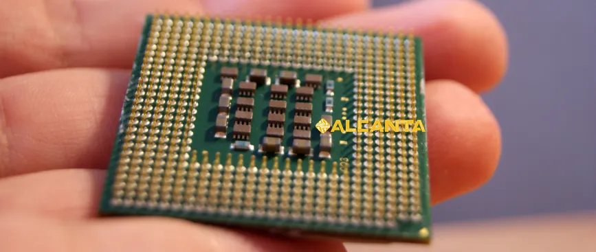
Flip Chip BGA Substrate is a sophisticated electronic packaging technology that offers numerous advantages over traditional packaging methods. At its core, Flip Chip BGA Substrate involves flipping semiconductor chips upside down and directly bonding them onto the substrate using solder bumps or micro-bumps. This inverted configuration enables direct electrical connections between the chip and the substrate, eliminating the need for wire bonds and allowing for shorter interconnection lengths.
The structure of a Flip Chip BGA Substrate typically consists of several layers, including a substrate layer, a redistribution layer (RDL), and solder bumps or micro-bumps. The substrate layer serves as the foundation onto which the semiconductor chips are attached, providing mechanical support and electrical pathways. The RDL redistributes the electrical signals from the input/output (I/O) pads of the chip to the corresponding solder bumps or micro-bumps, ensuring proper connectivity.
In electronic packaging, Flip Chip BGA Substrate plays a crucial role in enhancing device performance, reliability, and miniaturization. Unlike traditional packaging techniques such as wire bonding, Flip Chip BGA Substrate offers superior electrical and thermal performance due to its shorter interconnection lengths and improved heat dissipation capabilities. This makes it particularly suitable for high-speed and high-power applications where signal integrity and thermal management are critical.
Furthermore, Flip Chip BGA Substrate enables increased component density, allowing for the integration of more functionality into smaller form factors. Its compact design also facilitates the development of thinner and lighter electronic devices, making it ideal for applications where space constraints are a concern.
Compared to other packaging technologies like through-hole mounting and surface mount technology (SMT), Flip Chip BGA Substrate offers higher interconnection densities, better electrical performance, and enhanced reliability. Its ability to accommodate fine pitch interconnects and complex integrated circuits makes it a preferred choice for advanced electronic systems.
In summary, Flip Chip BGA Substrate represents a significant advancement in electronic packaging, offering superior performance, reliability, and miniaturization capabilities compared to traditional packaging methods. Its role in electronic packaging is paramount, driving innovation and enabling the development of next-generation electronic devices.
Differences Between Flip Chip BGA Substrate and BGA
Flip Chip BGA Substrate and traditional BGA packaging are both popular methods for mounting semiconductor chips onto substrates, but they differ significantly in their construction, performance, and applications.
Similarities:
Both Flip Chip BGA Substrate and BGA involve attaching semiconductor chips onto substrates using solder connections.
They both provide electrical connections between the chips and the substrate, facilitating the transfer of signals and power.
Both packaging methods are widely used in the electronics industry for various applications, including consumer electronics, telecommunications, automotive systems, and medical devices.
Differences:
1. Mounting Orientation: The most noticeable difference between Flip Chip BGA Substrate and BGA is the orientation of the semiconductor chips. In Flip Chip BGA Substrate, the chips are flipped upside down and directly bonded onto the substrate, whereas in traditional BGA, the chips are mounted right-side-up with their bonding pads facing downwards.
2. Interconnection Method: Flip Chip BGA Substrate utilizes solder bumps or micro-bumps for direct chip-to-substrate connections, resulting in shorter interconnection lengths and improved electrical performance. In contrast, BGA relies on wire bonds or solder balls to establish connections between the chip and the substrate, which may introduce longer interconnection lengths and higher parasitic capacitance.
3. Space Utilization: Flip Chip BGA Substrate offers higher component density and better space utilization compared to traditional BGA packaging. By eliminating the need for wire bonds and allowing for finer pitch interconnects, Flip Chip technology enables the integration of more components into a smaller footprint, making it ideal for applications where space is limited.
4. Thermal Management: Flip Chip BGA Substrate typically offers superior thermal performance compared to BGA packaging. The direct attachment of chips onto the substrate facilitates efficient heat dissipation, reducing thermal resistance and improving device reliability. This makes Flip Chip technology particularly suitable for high-power applications where thermal management is critical.
Advantages of Flip Chip Technology:
– Improved Electrical Performance: Flip Chip BGA Substrate offers shorter interconnection lengths, lower parasitic capacitance, and higher signal integrity compared to BGA packaging, leading to better electrical performance.
– Enhanced Thermal Management: The direct chip-to-substrate attachment in Flip Chip technology enables more efficient heat dissipation, resulting in lower operating temperatures and improved reliability.
– Higher Component Density: Flip Chip BGA Substrate allows for finer pitch interconnects and tighter component spacing, enabling the integration of more functionality into smaller form factors.
– Miniaturization: Flip Chip technology facilitates the development of thinner and lighter electronic devices, making it ideal for applications where size and weight constraints are crucial.
Applicable Scenarios:
Flip Chip BGA Substrate is well-suited for high-performance electronic systems where compact size, high component density, and superior electrical and thermal performance are essential. It is commonly used in applications such as high-speed data processing, telecommunications infrastructure, automotive electronics, and portable consumer devices. Additionally, Flip Chip technology is favored in applications where reliability and longevity are critical, such as aerospace and medical devices, due to its robust construction and enhanced thermal management capabilities.
Applications of Flip Chip BGA Substrate
Flip Chip BGA Substrate finds extensive applications across a diverse range of electronic devices, owing to its superior performance, reliability, and miniaturization capabilities. Let’s explore some of its key applications in various industries:
1. High-Performance Computing (HPC): In the field of high-performance computing, such as supercomputers, data centers, and server farms, Flip Chip BGA Substrate plays a critical role in enabling faster data processing, higher computational power, and improved energy efficiency. The compact design and efficient thermal management of Flip Chip technology allow for the integration of multiple high-speed processors, memory modules, and other components into densely packed systems, delivering unparalleled performance for complex computational tasks.
2. Communication Equipment: Flip Chip BGA Substrate is widely used in communication equipment, including routers, switches, base stations, and optical networking devices. Its high-speed signal transmission capabilities, low power consumption, and compact form factor make it ideal for supporting the high-bandwidth requirements of modern communication networks. Flip Chip technology enables the integration of advanced RF components, digital signal processors, and high-speed interfaces, ensuring reliable and efficient communication across various wired and wireless platforms.
3. Consumer Electronics: Flip Chip BGA Substrate is ubiquitous in consumer electronics products such as smartphones, tablets, laptops, and wearable devices. Its compact size, lightweight design, and robust construction make it well-suited for portable and handheld applications where space constraints and durability are paramount. Flip Chip technology enables the integration of advanced processors, graphics chips, sensors, and memory modules into sleek and slim devices, delivering enhanced performance, longer battery life, and seamless user experiences.
4. Automotive Electronics: In the automotive industry, Flip Chip BGA Substrate is used in a wide range of applications, including advanced driver-assistance systems (ADAS), infotainment systems, engine control units (ECUs), and automotive radar systems. Its ruggedized construction, high-temperature tolerance, and vibration resistance make it suitable for harsh automotive environments. Flip Chip technology enables the integration of sophisticated electronic components with high reliability and long-term durability, enhancing vehicle safety, comfort, and performance.
5. Medical Devices: Flip Chip BGA Substrate plays a crucial role in medical devices and equipment, including diagnostic imaging systems, patient monitoring devices, and implantable medical devices. Its compact design, high signal integrity, and biocompatibility make it ideal for medical applications where precision, reliability, and patient safety are paramount. Flip Chip technology enables the miniaturization of medical devices, allowing for non-invasive procedures, remote monitoring, and personalized healthcare solutions.
Overall, Flip Chip BGA Substrate is a versatile and indispensable technology that drives innovation across various industries, enabling the development of advanced electronic devices with superior performance, reliability, and functionality. Its widespread adoption in high-performance computing, communication equipment, consumer electronics, automotive electronics, and medical devices underscores its significant impact on modern technology and society.
Future Trends of Flip Chip BGA Substrate
As technology continues to evolve at a rapid pace, the future of Flip Chip BGA Substrate holds exciting prospects for further advancements and innovations. Here are some key trends and development directions to consider:
1. Miniaturization and Integration: One of the main trends in the future of Flip Chip BGA Substrate is the ongoing push towards miniaturization and integration. As electronic devices become increasingly compact and portable, there will be a growing demand for Flip Chip technology to enable the integration of more functionality into smaller form factors. Manufacturers will continue to explore ways to shrink the size of Flip Chip BGA Substrate assemblies while maintaining or improving performance.
2. High-Speed and High-Frequency Applications: With the proliferation of high-speed data communication, 5G technology, and emerging applications such as artificial intelligence (AI) and Internet of Things (IoT), there will be a greater need for Flip Chip BGA Substrate solutions capable of supporting high-frequency signals and high-speed data transmission. Future developments may focus on optimizing the design and materials of Flip Chip assemblies to minimize signal loss and electromagnetic interference (EMI).
3. Advanced Packaging Technologies: The future of Flip Chip BGA Substrate will likely see continued integration with other advanced packaging technologies such as system-in-package (SiP), 3D integration, and heterogeneous integration. These advanced packaging approaches enable the stacking and integration of multiple components, including processors, memory, sensors, and RF modules, within a single package, offering enhanced functionality and performance in a smaller footprint.
4. Flexible and Stretchable Electronics: Another emerging trend in the future of Flip Chip BGA Substrate is the development of flexible and stretchable electronics. These technologies enable the creation of bendable and conformable electronic devices for applications in wearable electronics, healthcare monitoring, and flexible displays. Flip Chip BGA Substrate solutions optimized for flexible substrates and stretchable interconnects will be crucial in enabling the realization of these futuristic applications.
5. Advanced Materials and Processes: Future developments in Flip Chip BGA Substrate will likely involve the adoption of advanced materials and manufacturing processes to meet evolving market demands. This may include the use of novel substrate materials with improved electrical and thermal properties, as well as the development of innovative bonding techniques and underfill materials to enhance reliability and performance.
6. Enhanced Reliability and Durability: As electronic devices become more integrated into our daily lives and mission-critical applications, there will be an increasing emphasis on enhancing the reliability and durability of Flip Chip BGA Substrate assemblies. Future trends may include the implementation of advanced testing and inspection techniques, as well as the integration of self-diagnostic features and predictive maintenance capabilities to improve reliability and prevent unexpected failures.
In summary, the future of Flip Chip BGA Substrate holds tremendous potential for innovation and growth, driven by the need for smaller, faster, and more reliable electronic devices. By embracing emerging technologies, materials, and manufacturing processes, manufacturers can continue to push the boundaries of Flip Chip technology and meet the evolving demands of the market.
FAQs about flip chip bga substrate
The substrate of the flip chip package typically consists of a base material, such as organic substrates (e.g., FR-4), ceramic substrates (e.g., alumina or aluminum nitride), or laminate materials (e.g., BT resin), onto which the semiconductor chips are directly bonded using solder bumps or micro-bumps.
No, flip chip and BGA (Ball Grid Array) are not the same. Flip chip refers to a packaging technology where semiconductor chips are flipped upside down and directly bonded onto a substrate using solder bumps or micro-bumps, whereas BGA is a type of packaging where semiconductor chips are mounted right-side-up with their bonding pads facing downwards and connected to the substrate via solder balls arranged in a grid pattern.
The material used in flip chip technology varies depending on the specific requirements of the application, but common materials include metals such as copper, aluminum, or gold for the interconnects, and solder materials such as tin-lead (SnPb) or lead-free alloys (e.g., SAC305) for the solder bumps or micro-bumps.
The substrate of a BGA typically consists of a base material, similar to that of flip chip packages, such as organic substrates, ceramic substrates, or laminate materials. In BGA packaging, semiconductor chips are mounted right-side-up with their bonding pads facing downwards and connected to the substrate via solder balls arranged in a grid pattern.

