
Embracing Eco-Friendly Electronics: The Rise of Organic PCB Substrates
In today’s rapidly evolving electronics industry, the emergence of organic PCB substrate technology marks a significant milestone. This innovative approach not only revolutionizes traditional manufacturing processes but also underscores a crucial shift towards sustainability and performance. As the demand for environmentally friendly solutions continues to surge, organic PCB substrates have garnered immense attention for their unparalleled benefits. With their ability to deliver both high performance and eco-friendliness, these substrates are reshaping the landscape of PCB manufacturing. In this era of heightened environmental consciousness, the adoption of organic PCB substrates represents a proactive step towards reducing carbon footprint while ensuring optimal functionality in electronic devices.
What is Organic PCB Substrate?
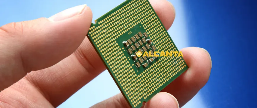
Organic PCB substrate refers to a type of printed circuit board (PCB) material that utilizes organic compounds as its base material. Unlike traditional substrates such as fiberglass-reinforced epoxy resin (FR-4), which primarily consist of inorganic materials, organic PCB substrates incorporate organic polymers and resins. These organic materials, often derived from sources like cellulose or polyimide, offer distinct advantages in PCB manufacturing.
Composition:
Organic PCB substrates typically comprise layers of organic polymers laminated together with conductive traces etched onto their surfaces. These polymers may include polyethylene terephthalate (PET), polyimide (PI), or epoxy-based resins. The composition may also include additives such as flame retardants or fillers to enhance specific properties like flame resistance or mechanical strength.
Benefits of Organic Materials:
Using organic materials in PCB manufacturing offers several advantages. Firstly, organic substrates tend to have better flexibility and thermal stability compared to inorganic alternatives. This flexibility allows for more intricate PCB designs and makes organic substrates suitable for applications where bending or deformation is expected. Additionally, organic materials often exhibit lower dielectric constants and dissipation factors, leading to improved signal integrity and reduced signal loss in high-frequency applications.
Comparison with Traditional Alternatives:
When compared to traditional substrates like FR-4, organic PCB substrates offer distinct advantages. While FR-4 is known for its rigidity and mechanical strength, organic substrates excel in flexibility and thermal management. Organic materials also tend to have better resistance to environmental factors such as moisture and chemicals, making them suitable for harsh operating conditions. Furthermore, organic PCB substrates contribute to sustainability efforts due to their biodegradability and reduced environmental impact during production.
In summary, organic PCB substrates represent a modern approach to PCB manufacturing, offering enhanced performance, flexibility, and environmental sustainability compared to traditional alternatives.
Advantages of Organic PCB Substrate
1. Enhanced Flexibility and Durability:
Organic PCB substrates offer superior flexibility compared to traditional alternatives like FR-4. This flexibility allows for the creation of PCBs with intricate designs and shapes, making them ideal for applications where space constraints or bending requirements are prevalent. Additionally, organic substrates exhibit enhanced durability, resisting cracking or damage from mechanical stress, which is crucial for portable electronic devices or products subjected to frequent handling.
2. Improved Thermal Management:
Organic materials possess excellent thermal management properties, enabling efficient heat dissipation from electronic components. This is particularly beneficial in high-power applications or densely packed electronic devices where thermal issues can affect performance and reliability. Organic PCB substrates help prevent overheating by effectively channeling heat away from critical components, thereby extending the lifespan of electronic devices and reducing the risk of thermal-induced failures.
3. Environmental Sustainability:
One of the most significant advantages of organic PCB substrates is their environmental sustainability. Unlike traditional substrates, which often contain non-biodegradable or hazardous materials, organic materials are derived from renewable sources and are biodegradable. This aligns with the growing demand for eco-friendly electronic products and manufacturing processes, contributing to efforts to reduce waste and minimize environmental impact.
4. Reduced Carbon Footprint:
By opting for organic PCB substrates, manufacturers can significantly reduce the carbon footprint associated with PCB manufacturing. Organic materials typically have lower energy requirements and produce fewer greenhouse gas emissions during production compared to inorganic alternatives. Additionally, the biodegradability of organic substrates means they have a smaller environmental footprint throughout their lifecycle, from production to disposal.
5. Cost-Effectiveness and Efficient Manufacturing Processes:
Organic PCB substrates offer cost-effective solutions for PCB manufacturing. Their compatibility with modern fabrication techniques, such as inkjet printing or roll-to-roll processing, streamlines production processes and reduces manufacturing costs. Furthermore, the abundance of organic materials in nature contributes to lower material costs compared to inorganic substrates, making organic PCBs a cost-effective choice for electronic manufacturers without compromising performance or quality.
In conclusion, the advantages of organic PCB substrates extend beyond performance enhancements to encompass environmental sustainability, cost-effectiveness, and efficient manufacturing processes, making them an ideal choice for modern electronics applications.
Key Features of Organic PCB Substrate
1. High Dielectric Constant and Insulation Properties:
Organic PCB substrates exhibit a high dielectric constant, which is crucial for effectively storing and transmitting electrical energy within the circuit. This property ensures optimal signal propagation and minimizes signal loss, especially in high-frequency applications. Additionally, organic materials provide excellent insulation, preventing electrical leakage and ensuring reliable operation of electronic devices.
2. Compatibility with Advanced Fabrication Techniques:
Organic PCB substrates are highly compatible with advanced fabrication techniques such as additive manufacturing, inkjet printing, and flexible electronics manufacturing processes. This compatibility enables the creation of complex PCB designs with intricate features, including fine traces, microvias, and embedded components. Manufacturers can leverage these advanced techniques to achieve higher levels of integration, miniaturization, and functionality in electronic devices.
3. Excellent Signal Integrity and Impedance Control:
Organic materials offer superior signal integrity and impedance control, essential for maintaining the integrity of high-speed digital signals and analog signals in electronic circuits. Organic PCB substrates have low loss tangent and minimal dispersion, ensuring minimal distortion and signal degradation. This results in improved data transmission accuracy, reduced electromagnetic interference (EMI), and enhanced overall performance of electronic systems.
4. Resistance to Moisture, Chemicals, and Mechanical Stress:
Organic PCB substrates exhibit robust resistance to moisture, chemicals, and mechanical stress, enhancing the reliability and longevity of electronic devices. Organic materials, such as polyimide or epoxy-based resins, form protective barriers that shield circuitry from environmental factors, including humidity, corrosive substances, and physical impact. This resistance ensures stable operation of electronic devices even in challenging operating conditions, making organic PCB substrates ideal for applications in harsh environments or demanding industrial settings.
In summary, the key features of organic PCB substrates, including their high dielectric constant, compatibility with advanced fabrication techniques, excellent signal integrity, and resistance to environmental factors, make them a preferred choice for a wide range of electronic applications, from consumer electronics to aerospace and automotive systems.
Selecting the Right PCB Substrate
1. Understanding the Specific Requirements of the Application:
Selecting the right PCB substrate begins with a thorough understanding of the application’s specific requirements. Factors such as operating environment, desired lifespan, thermal constraints, and performance expectations play a crucial role in determining the optimal substrate material. For example, aerospace or automotive applications may require substrates with high temperature resistance and reliability, while consumer electronics may prioritize flexibility and cost-effectiveness.
2. Evaluating Factors such as Thermal Performance, Electrical Properties, and Reliability:
Thermal performance, electrical properties, and reliability are critical factors to consider when selecting a PCB substrate. Thermal conductivity and dissipation properties are essential for managing heat generated by electronic components and preventing thermal-induced failures. Electrical properties, including dielectric constant, loss tangent, and impedance control, directly impact signal integrity and performance. Reliability considerations encompass mechanical strength, resistance to environmental stressors, and long-term stability to ensure consistent operation over the product’s lifespan.
3. Considering Environmental Regulations and Sustainability Goals:
Environmental regulations and sustainability goals are increasingly influencing PCB substrate selection decisions. Manufacturers must prioritize materials that comply with regulations such as RoHS (Restriction of Hazardous Substances) and REACH (Registration, Evaluation, Authorization, and Restriction of Chemicals) to ensure compliance with environmental standards and minimize environmental impact. Additionally, considering sustainability goals involves opting for materials with minimal environmental footprint, such as biodegradable or recyclable substrates, to support eco-friendly manufacturing practices.
4. Collaborating with Reputable Suppliers like Kyocera for Quality Assurance:
Collaborating with reputable suppliers like Kyocera is paramount to ensuring quality assurance and reliability in PCB substrate selection. Established suppliers with a track record of excellence offer expertise in material selection, manufacturing processes, and quality control measures. Partnering with such suppliers enables access to high-quality materials, customized solutions, and technical support throughout the product development lifecycle. Moreover, reputable suppliers like Kyocera prioritize innovation and sustainability, aligning with the industry’s evolving needs and environmental responsibilities.
By carefully considering these factors and collaborating with trusted suppliers, manufacturers can confidently select the right PCB substrate that meets the unique requirements of their application while ensuring optimal performance, reliability, and sustainability.
Are PCBs Biodegradable?
1. Exploring the Biodegradability of Organic PCB Substrates:
Organic PCB substrates, derived from natural sources such as cellulose or polyimide, have demonstrated biodegradability under certain conditions. Unlike traditional substrates that contain non-biodegradable materials like fiberglass and epoxy resin, organic substrates break down over time through microbial action and environmental processes. This inherent biodegradability reduces the environmental impact of PCB disposal and contributes to sustainable waste management practices.
2. Discussing the Importance of Eco-Friendly Disposal and Recycling Practices:
The disposal of PCBs, whether organic or traditional, poses environmental challenges due to their complex composition and potential for toxic elements. Implementing eco-friendly disposal and recycling practices is crucial to minimize environmental pollution and resource depletion. Recycling PCBs allows for the recovery of valuable materials like copper and gold, reducing the need for virgin resources and minimizing waste generation. Additionally, proper disposal methods, such as incineration in controlled environments or chemical treatment, can mitigate the release of harmful substances into the environment.
3. Highlighting the Role of Innovation in Developing Sustainable Electronic Solutions:
Innovation plays a pivotal role in developing sustainable electronic solutions, including biodegradable PCB substrates. Ongoing research and development efforts focus on improving the biodegradability, performance, and cost-effectiveness of organic materials for PCB manufacturing. Advanced manufacturing techniques, such as green chemistry processes and additive manufacturing, enable the production of eco-friendly PCBs with enhanced functionality and reliability. Furthermore, collaborations between industry stakeholders, academia, and government agencies drive the adoption of sustainable practices and promote the development of environmentally responsible electronic products.
In conclusion, while PCBs have historically posed challenges in terms of environmental impact, the emergence of biodegradable organic substrates, coupled with eco-friendly disposal and recycling practices, offers promising solutions. By embracing innovation and sustainability, the electronics industry can transition towards a more environmentally conscious future, where PCBs play a vital role in advancing technology while minimizing their ecological footprint.
Kyocera’s Contribution to Organic PCB Substrates
1. Introducing Kyocera’s Expertise in Organic Substrate Technology:
Kyocera, a renowned leader in electronics manufacturing, boasts extensive expertise in organic substrate technology. Leveraging years of research and development, Kyocera has pioneered advancements in organic materials and manufacturing processes, positioning itself as a trusted innovator in the field of PCB substrates. Through a combination of cutting-edge technologies and engineering prowess, Kyocera continues to push the boundaries of what’s possible in organic PCB substrate design and production.
2. Showcasing Kyocera’s Range of Organic PCB Substrate Products:
Kyocera offers a diverse range of organic PCB substrate products tailored to meet the evolving needs of modern electronics applications. These substrates are meticulously designed and engineered to deliver exceptional performance, reliability, and environmental sustainability. From flexible and high-density interconnect (HDI) boards to specialized substrates for automotive, aerospace, and consumer electronics, Kyocera provides solutions that empower customers to achieve their goals with confidence.
3. Discussing Kyocera’s Commitment to Environmental Stewardship and Technological Innovation:
Environmental stewardship and technological innovation are at the core of Kyocera’s corporate philosophy. Recognizing the importance of sustainable practices in today’s world, Kyocera is dedicated to minimizing its environmental footprint across all aspects of its operations, including PCB substrate manufacturing. By prioritizing the use of eco-friendly materials, reducing energy consumption, and implementing waste reduction strategies, Kyocera demonstrates its commitment to preserving the planet for future generations.
Furthermore, Kyocera’s relentless pursuit of technological innovation drives the development of organic PCB substrates that not only meet but exceed industry standards. By investing in research, collaborating with industry partners, and leveraging its vast resources, Kyocera continuously delivers solutions that push the boundaries of performance, reliability, and sustainability in electronic manufacturing.
In summary, Kyocera’s contributions to organic PCB substrates extend beyond product offerings to encompass a legacy of expertise, innovation, and environmental responsibility. As a trusted partner in the electronics industry, Kyocera remains dedicated to empowering customers with cutting-edge solutions that drive progress while preserving the planet.
FAQs about organic pcb substrate
The best substrate for a PCB depends on the specific requirements of the application. Factors such as thermal performance, electrical properties, reliability, and environmental considerations influence substrate selection.
An organic PCB refers to a printed circuit board (PCB) that utilizes organic compounds, such as polymers and resins, as its base material instead of traditional inorganic materials like fiberglass-reinforced epoxy resin (FR-4). Organic PCBs offer advantages such as enhanced flexibility, thermal management, and environmental sustainability.
Selecting a PCB substrate involves understanding the application’s requirements, evaluating factors like thermal performance, electrical properties, and reliability, considering environmental regulations and sustainability goals, and collaborating with reputable suppliers for quality assurance.
PCBs can be biodegradable, particularly those made from organic materials. Organic PCB substrates have demonstrated biodegradability under certain conditions, contributing to sustainable waste management practices. However, the biodegradability of PCBs depends on the specific materials used and the disposal methods employed.

