
From Chips to Systems: The Importance of Packaging Substrates
In the intricate realm of semiconductor technology, packaging substrates stand as unsung heroes, enabling the seamless integration of microelectronic components. These substrates serve as the foundation upon which delicate semiconductor chips are mounted, connecting them to the broader electronic system. Beyond mere physical support, packaging substrates play a pivotal role in ensuring the functionality and reliability of electronic devices. They facilitate electrical pathways, dissipate heat, and safeguard against environmental stresses, thus safeguarding the integrity of the entire system. Understanding the significance of packaging substrates unveils the cornerstone of modern electronics, where every intricate circuit and intricate connection finds its home and purpose.
Understanding Packaging Substrates:
Packaging substrates serve as the vital bridge between semiconductor chips and the broader electronic system. They are essentially the foundation upon which delicate semiconductor components are mounted, providing structural integrity and electrical connectivity. Their significance in semiconductor packaging cannot be overstated, as they dictate the performance, reliability, and thermal management of electronic devices.
Types of Packaging Substrates
- Organic Substrates: These substrates, typically made of materials like FR-4 or polyimide, offer cost-effective solutions for packaging. They are widely used in consumer electronics and offer moderate thermal performance.
- Flip Chip Substrates: Designed for high-density packaging, flip chip substrates allow direct mounting of semiconductor chips without the need for wire bonding. They provide excellent electrical performance and are commonly used in applications requiring high-speed data transmission.
- Semiconductor Packaging Substrates: These substrates are specifically tailored for semiconductor packaging, offering enhanced electrical connectivity and thermal dissipation. They are crucial for advanced semiconductor devices requiring precise signal transmission and thermal management.
Materials and Properties
Packaging substrates can be fabricated from various materials, each with distinct properties:
- FR-4: A common choice for organic substrates, FR-4 offers good electrical insulation and mechanical strength, making it suitable for standard electronic applications.
- Polyimide: Known for its flexibility and high-temperature resistance, polyimide substrates are ideal for applications demanding ruggedness and reliability.
- Ceramics: Ceramic substrates provide excellent thermal conductivity, making them suitable for high-power applications where efficient heat dissipation is critical.
- Metal-Core Substrates: These substrates feature a metal core sandwiched between layers of dielectric material, offering superior thermal performance and mechanical stability.
Understanding the properties of these materials is crucial for designing packaging substrates that meet the specific requirements of diverse semiconductor applications, ensuring optimal performance and reliability.
Functionality and Purpose of Package Substrates:
Package substrates play multifaceted roles within semiconductor devices, crucial for their functionality, reliability, and overall performance.
Primary Functions
- Electrical Connections: Package substrates serve as the platform for interconnecting semiconductor chips with external components, such as printed circuit boards (PCBs) or other chips. Through intricate routing of conductive traces, they establish electrical pathways that facilitate signal transmission, power distribution, and data processing. These pathways ensure seamless communication between various components within the electronic system, enabling its proper operation.
- Thermal Management: Efficient heat dissipation is essential for maintaining the optimal operating temperature of semiconductor devices, as excessive heat can degrade performance and reliability. Package substrates play a critical role in thermal management by providing a pathway for heat to dissipate from the semiconductor chip to the surrounding environment. By incorporating thermally conductive materials and strategically designed vias, package substrates help conduct heat away from the chip, ensuring its longevity and reliability.
- Mechanical Support: Semiconductor chips are delicate components that require robust support to withstand mechanical stresses encountered during handling, assembly, and operation. Package substrates offer mechanical support to the chip, protecting it from physical damage and ensuring its structural integrity. Additionally, they provide a secure mounting platform for the chip within the semiconductor package, preventing displacement or misalignment.
Illustrative Examples
- Mobile Devices: In smartphones and tablets, package substrates enable the integration of multiple semiconductor chips, such as processors, memory modules, and sensors, into compact and lightweight assemblies. By facilitating efficient electrical connections and thermal management, package substrates contribute to the seamless operation of these devices, enhancing their performance and reliability.
- Automotive Electronics: Package substrates play a vital role in automotive electronic systems, where reliability and durability are paramount. In advanced driver assistance systems (ADAS) and engine control units (ECUs), package substrates ensure robust electrical connections and effective thermal dissipation, allowing semiconductor devices to operate reliably in harsh environmental conditions, such as temperature variations and vibrations.
- Data Centers: In high-performance computing applications, such as data centers and cloud servers, package substrates enable the integration of powerful processors and memory modules, optimizing data processing capabilities. Through efficient electrical connections and thermal management, package substrates contribute to the uninterrupted operation of these critical infrastructure components, minimizing downtime and ensuring data reliability.
Comparing Substrate and Package
In semiconductor terminology, the terms “substrate” and “package” refer to distinct yet interconnected components crucial for the assembly and functionality of semiconductor devices.
Differentiation between Substrate and Package
- Substrate: The substrate is the foundational layer upon which semiconductor components are mounted. It typically consists of a thin, flat material, such as silicon, ceramic, or organic substrate. The substrate provides structural support and electrical connectivity for semiconductor chips, often featuring intricate wiring patterns and vias for signal transmission. In essence, the substrate serves as the immediate platform for the integration of semiconductor devices.
- Package: The package, on the other hand, encapsulates and protects the semiconductor chip and its substrate. It is an external casing that shields the delicate semiconductor components from environmental factors, such as moisture, dust, and physical damage. Packages come in various forms, including ceramic packages, plastic packages, and ball grid arrays (BGAs). Additionally, packages may include features such as heat sinks, lids, and lead frames to enhance thermal dissipation and mechanical robustness.
Complementarity in Semiconductor Device Assembly
Substrates and packages work in tandem to ensure the functionality, reliability, and performance of semiconductor devices:
- Electrical Connectivity: Substrates provide the necessary electrical pathways for interconnecting semiconductor chips and external components, while packages encapsulate these connections, protecting them from external influences.
- Thermal Management: Substrates facilitate heat dissipation from the semiconductor chip to the surrounding environment, while packages incorporate thermal management features, such as heat sinks and thermal vias, to further enhance heat dissipation and maintain optimal operating temperatures.
- Mechanical Support: Substrates offer mechanical support and stability to semiconductor chips, preventing physical damage and ensuring proper alignment within the package. Packages, in turn, provide additional mechanical protection and structural integrity to the assembled semiconductor device.
Interplay between Substrate Design and Package Architecture
The design of the substrate directly influences the overall package architecture and performance of the semiconductor device:
- Integration: Substrate design considerations, such as layout, material selection, and routing topology, influence the placement and arrangement of semiconductor chips within the package. This, in turn, affects the overall size, form factor, and functionality of the packaged device.
- Signal Integrity: Substrate design parameters, including trace impedance, signal propagation delay, and electromagnetic interference (EMI) mitigation techniques, impact the electrical performance and signal integrity of the packaged semiconductor device.
- Thermal Considerations: Substrate materials with high thermal conductivity and efficient heat dissipation properties contribute to improved thermal performance within the package. This enables higher power densities and prolonged device lifespan, enhancing overall reliability.
In essence, the interplay between substrate design and package architecture is integral to achieving optimal performance, reliability, and functionality in semiconductor devices. By synergistically addressing electrical, thermal, and mechanical requirements, substrates and packages collectively enable the realization of advanced semiconductor technologies.
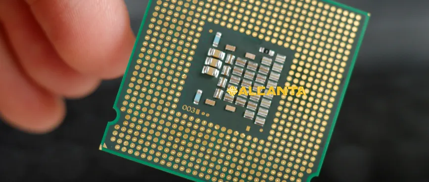
The Anatomy of Chip Packaging Substrates:
Chip packaging substrates consist of several key components meticulously designed to facilitate the integration of semiconductor chips and other electronic components while ensuring optimal performance and reliability.
Detailed Examination of Substrate Components
- Base Material: The base material of chip packaging substrates can vary depending on the application requirements. Common materials include FR-4 (fiberglass-reinforced epoxy), polyimide, ceramic, and metal-core substrates. Each material offers unique properties such as electrical insulation, thermal conductivity, and mechanical strength.
- Conductive Traces and Vias: Conductive traces, typically made of copper, are patterned on the substrate surface to create electrical pathways between semiconductor chips and external components. Vias, which are plated holes in the substrate, provide vertical connections between different substrate layers, enabling multilayer routing and signal transmission.
- Dielectric Layers: Dielectric layers insulate conductive traces and provide mechanical support to the substrate. These layers are essential for preventing short circuits and ensuring signal integrity within the substrate.
- Solder Mask: Solder mask is applied over the substrate surface to protect conductive traces from environmental factors and prevent unintended solder bridging during assembly. It also helps to define the solderable areas for attaching semiconductor chips and other components.
Overview of Layout and Structure
Chip packaging substrates are typically designed in a layered structure, with each layer serving specific functions:
- Top Layer: This layer contains the solder pads and conductive traces for connecting semiconductor chips and external components. It also includes alignment marks and fiducials for precise chip placement during assembly.
- Inner Layers: These layers consist of additional conductive traces and vias, enabling complex routing and interconnectivity within the substrate. The number of inner layers varies depending on the complexity of the substrate design and the required signal density.
- Bottom Layer: Similar to the top layer, the bottom layer contains solder pads and conductive traces for connecting to external components such as printed circuit boards (PCBs) or other substrates. It may also include features for heat dissipation, such as thermal vias or copper planes.
Accommodation of Semiconductor Chips and Components
Chip packaging substrates are meticulously designed to accommodate the integration of semiconductor chips and other electronic components:
- Chip Mounting: Semiconductor chips are attached to the substrate surface using techniques such as wire bonding, flip chip bonding, or surface mount technology (SMT). The substrate provides a stable platform for mounting the chips and ensures proper electrical connections with the conductive traces.
- Component Integration: In addition to semiconductor chips, chip packaging substrates may also accommodate passive components such as resistors, capacitors, and inductors. These components are soldered or mounted onto the substrate to support various functionalities, such as decoupling, filtering, and signal conditioning.
By integrating semiconductor chips and electronic components onto a single substrate, chip packaging substrates enable the assembly of compact and highly integrated electronic systems, facilitating advancements in areas such as consumer electronics, automotive electronics, and telecommunications.
Applications and Uses of Packaging Substrates
Packaging substrates play a pivotal role across various industries, enabling the integration and functionality of semiconductor devices in a wide range of applications.
Comprehensive Overview of Applications
- Consumer Electronics: Packaging substrates are extensively utilized in consumer electronics such as smartphones, tablets, laptops, and wearable devices. They facilitate the integration of semiconductor chips and components, enabling compact and lightweight designs while ensuring high performance and reliability.
- Automotive Systems: In automotive electronics, packaging substrates are employed in critical systems such as engine control units (ECUs), advanced driver assistance systems (ADAS), infotainment systems, and vehicle-to-everything (V2X) communication modules. They enable the integration of semiconductor devices capable of withstanding harsh environmental conditions, temperature extremes, and mechanical vibrations.
- Medical Devices: Packaging substrates find applications in medical devices ranging from implantable pacemakers and defibrillators to diagnostic equipment and monitoring devices. They enable the integration of semiconductor chips for data processing, sensing, and communication, contributing to advancements in medical technology and patient care.
- Telecommunications: In telecommunications infrastructure, packaging substrates are used in networking equipment, base stations, routers, and optical communication systems. They facilitate the integration of high-speed data processing chips, memory modules, and networking components, enabling efficient data transmission and communication networks.
Exploration of Utilization in Various Industries
- Consumer Electronics: Packaging substrates in consumer electronics enable the miniaturization of electronic devices, allowing manufacturers to create sleek and portable products without compromising performance. For example, flip chip substrates are commonly used in smartphones to achieve high-density packaging and enhance signal transmission rates.
- Automotive Systems: In automotive systems, packaging substrates play a crucial role in ensuring the reliability and durability of electronic components in vehicles. Ceramic substrates are often used in automotive ECUs to withstand temperature fluctuations and harsh operating conditions, ensuring the continuous and reliable operation of critical systems.
- Medical Devices: Packaging substrates in medical devices enable the integration of advanced sensors, microcontrollers, and wireless communication modules, facilitating remote patient monitoring, diagnostic imaging, and therapeutic interventions. For example, organic substrates are utilized in wearable medical devices for their flexibility and lightweight properties, allowing for comfortable and unobtrusive monitoring of patient health metrics.
Case Studies of Innovative Uses
- Internet of Things (IoT) Devices: Packaging substrates are integral to IoT devices, enabling the seamless integration of sensors, microcontrollers, and wireless communication modules for data collection and transmission. For example, flexible substrates are utilized in smart wearable devices for their bendable and lightweight characteristics, enabling continuous health monitoring and activity tracking.
- 5G Infrastructure: In the deployment of 5G telecommunications networks, packaging substrates are employed in base stations and network equipment to support high-speed data transmission and low-latency communication. Advanced substrates with enhanced thermal conductivity and signal integrity are essential for maintaining the reliability and performance of 5G infrastructure in demanding operating environments.
- Edge Computing: Packaging substrates play a crucial role in edge computing devices, enabling localized data processing and analytics at the network edge. Substrates with integrated thermal management features are utilized to dissipate heat generated by high-performance processors, ensuring the efficient operation of edge computing systems in industrial automation, smart cities, and autonomous vehicles.
By facilitating the integration and functionality of semiconductor devices across diverse industries, packaging substrates drive innovation and advancement in technology, enabling the development of smarter, more efficient, and interconnected electronic systems.
FAQs About Packaging substrates
Substrate packaging refers to the integration of semiconductor chips onto a substrate, which serves as the foundational platform for electrical connections, thermal management, and mechanical support within a semiconductor device or package. It involves mounting the chips onto the substrate and connecting them to other components, such as printed circuit boards (PCBs), to form a functional electronic system.
The purpose of a package substrate is to provide structural support, electrical connectivity, and thermal management for semiconductor chips within a semiconductor package. It facilitates the integration of chips and other electronic components, ensuring proper functionality, reliability, and performance of the overall electronic system.
The substrate is the foundational layer upon which semiconductor chips are mounted, providing structural support and electrical connectivity within a semiconductor device. In contrast, the package encapsulates and protects the semiconductor chips and their substrate, shielding them from environmental factors and providing additional mechanical support. While the substrate is an internal component of the semiconductor device, the package is an external casing that houses the chips and substrate.
The substrate of chip packaging refers to the foundational layer upon which semiconductor chips are mounted and connected within a semiconductor package. It typically consists of materials such as silicon, ceramic, or organic substrate and features conductive traces, vias, and dielectric layers to facilitate electrical connections, thermal dissipation, and mechanical support for the chips. The substrate plays a crucial role in ensuring the functionality, reliability, and performance of the packaged semiconductor device.

