
Unlocking Efficiency: The Power of Dual Row QFN Packages
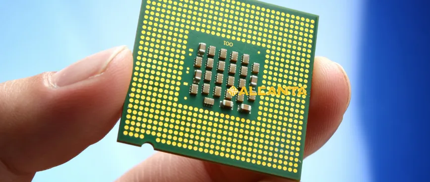
Dual Row QFN (Quad Flat No-Lead) Package is a type of surface mount semiconductor package featuring a lead frame with leads on all four sides, arranged in two rows. Unlike traditional single row QFN packages, dual row QFNs offer increased lead counts and improved electrical performance.
QFN packages, in general, have gained popularity due to their compact size, excellent thermal dissipation properties, and high electrical performance. They are widely used in various electronic applications where space-saving and efficient heat dissipation are critical factors. Now, let’s delve deeper into the specifics of dual row QFN packages and their unique advantages.
Types of QFN Packages
QFN (Quad Flat No-Lead) packages come in several variations, each designed to suit specific application requirements. Here are some common types:
Single Row QFN:
– Features a single row of leads around the perimeter of the package.
– Typically used in applications where space is limited and the number of I/Os is moderate.
– Offers simplified PCB layout and assembly.
Dual Row QFN:
– Consists of two rows of leads, effectively doubling the available I/O count compared to single row QFNs.
– Ideal for applications demanding higher I/O density while maintaining a compact footprint.
– Provides improved routing options on the PCB, enhancing signal integrity.
Exposed Pad QFN:
– Incorporates a central exposed thermal pad underneath the package.
– Enhances thermal dissipation by providing a direct path for heat transfer to the PCB.
– Suitable for power electronics and high-power applications requiring efficient heat management.
Bottom-terminated QFN (BT-QFN):
– Features leads or terminals on the bottom surface of the package instead of the sides.
– Enables direct soldering to the PCB, simplifying manufacturing processes.
– Offers enhanced electrical performance and reliability due to reduced parasitic effects.
Micro QFN:
– Miniaturized version of standard QFN packages, with reduced dimensions.
– Suited for applications where space constraints are extremely tight, such as wearables and mobile devices.
– Requires specialized assembly techniques and PCB design considerations.
Each type of QFN package has its unique features and advantages, catering to diverse application needs. The choice depends on factors like I/O requirements, thermal management, PCB layout constraints, and manufacturing considerations. Understanding these differences is crucial for selecting the most suitable package for a given application.
Advantages of QFN Packages
QFN (Quad Flat No-Lead) packages offer several advantages that make them highly desirable in various electronic applications:
1. Compact Size:
– QFN packages have a compact footprint due to their leadless design and surface mount configuration.
– They occupy less space on the PCB, allowing for smaller and more lightweight electronic devices.
– Ideal for applications where size and weight are critical considerations, such as portable electronics and IoT devices.
2. Excellent Thermal Performance:
– The exposed thermal pad on the underside of QFN packages facilitates efficient heat dissipation.
– Heat generated by the semiconductor device can quickly transfer through the thermal pad to the PCB, minimizing the risk of thermal damage.
– Enhanced thermal management capability makes QFN packages suitable for high-power applications and environments with elevated operating temperatures.
3. Enhanced Electrical Characteristics:
– QFN packages exhibit low inductance and capacitance, leading to improved electrical performance.
– Shorter interconnect lengths between the semiconductor die and the PCB result in reduced parasitic effects and improved signal integrity.
– This translates to higher-speed operation, lower power consumption, and better overall reliability in electronic circuits.
4. Robust Mechanical Durability:
– The absence of traditional leads or pins reduces the risk of mechanical failure due to bending or solder joint fatigue.
– QFN packages offer greater resistance to mechanical stresses such as vibration and shock, making them suitable for rugged applications and harsh operating environments.
5. Cost-Effective Manufacturing:
– QFN packages are compatible with standard surface mount assembly processes, leading to cost savings in manufacturing.
– Their simplified design and leadless construction contribute to higher yields and lower defect rates during production.
– Additionally, the absence of leads eliminates the need for lead forming and trimming processes, further streamlining manufacturing workflows.
In summary, QFN packages excel in electronic applications due to their compact size, superior thermal performance, enhanced electrical characteristics, mechanical durability, and cost-effective manufacturing. These advantages make them a preferred choice for a wide range of consumer, industrial, automotive, and telecommunications products.
Disadvantages of QFN Packages
While QFN (Quad Flat No-Lead) packages offer numerous advantages, they are not without their limitations and challenges:
1. Difficulty in Rework:
– QFN packages are challenging to rework or repair once soldered to the PCB due to their leadless design.
– Accessing and removing the package without damaging surrounding components or the PCB can be complex and time-consuming.
– Reworking QFN packages may require specialized equipment and expertise, increasing the cost and complexity of the process.
2. Limited Flexibility:
– The rigid construction of QFN packages offers limited flexibility compared to packages with leads or pins.
– Flexibility is crucial in applications where components may undergo mechanical stress or thermal expansion, potentially leading to reliability issues.
– Designers must carefully consider the mechanical requirements of the application and select alternative packaging options if flexibility is a concern.
3. Moisture Sensitivity:
– QFN packages, especially those with exposed thermal pads, are susceptible to moisture ingress during storage or handling.
– Moisture can lead to delamination, solder joint failures, or electrical performance degradation, particularly in environments with temperature cycling.
– Proper moisture-sensitive handling precautions and storage conditions are necessary to mitigate the risk of damage to QFN packages.
4. Risk of Solder Bridging:
– The closely spaced leads or pads in QFN packages increase the risk of solder bridging during assembly.
– Solder bridging occurs when solder inadvertently bridges adjacent leads or pads, causing short circuits and reliability issues.
– Careful stencil design, solder paste application, and reflow profile optimization are essential to minimize the occurrence of solder bridging during PCB assembly.
5. Inspection Challenges:
– The absence of visible leads or pins in QFN packages makes visual inspection of solder joints more challenging.
– Automated optical inspection (AOI) systems may have difficulty accurately inspecting QFN solder joints, leading to potential defects going undetected.
– Inspection techniques such as X-ray inspection or infrared thermography may be necessary to ensure the quality and reliability of QFN solder joints.
In conclusion, while QFN packages offer significant advantages in size, thermal performance, and electrical characteristics, they also present challenges such as difficulty in rework, limited flexibility, moisture sensitivity, risk of solder bridging, and inspection challenges. Designers and manufacturers must carefully weigh these factors and implement appropriate mitigation strategies to ensure the successful integration and reliability of QFN packages in electronic assemblies.
Comparison: QFN vs. QFP Packages
QFN (Quad Flat No-Lead) and QFP (Quad Flat Package) are two common types of surface mount semiconductor packages, each with distinct characteristics and applications. Let’s explore the fundamental differences between these two package types:
1. Package Size:
– QFN packages typically have a smaller footprint compared to QFP packages due to their leadless design and surface mount configuration.
– The absence of leads or pins around the perimeter of the package allows for a more compact form factor in QFN packages, making them ideal for space-constrained applications.
2. Lead Count:
– QFP packages traditionally feature leads or pins extending from all four sides of the package in a dual in-line configuration.
– The lead count in QFP packages can range from several dozen to several hundred, depending on the specific package size and variant.
– In contrast, QFN packages may have fewer leads due to their leadless design, but they can offer higher lead densities, especially in dual row configurations.
3. Thermal Characteristics:
– QFN packages typically offer superior thermal performance compared to QFP packages.
– The exposed thermal pad on the underside of QFN packages provides a direct path for heat dissipation to the PCB, resulting in lower junction temperatures and improved reliability.
– QFP packages, with their enclosed design and larger body size, may exhibit higher thermal resistance and less efficient heat dissipation, especially in high-power applications.
4. Manufacturing Complexity:
– QFN packages generally involve simpler manufacturing processes compared to QFP packages.
– The leadless design of QFN packages eliminates the need for lead forming and trimming processes, streamlining assembly and reducing manufacturing costs.
– QFP packages, with their traditional leaded configuration, may require additional steps such as lead forming, insertion, and trimming, adding complexity and cost to the manufacturing process.
5. Application Flexibility:
– QFP packages are well-suited for applications requiring easy access to leads for testing, prototyping, or rework.
– The protruding leads or pins in QFP packages facilitate manual or automated handling during assembly and inspection processes.
– QFN packages, on the other hand, are preferred for applications where size, weight, and thermal performance are critical factors, such as mobile devices, automotive electronics, and high-density integrated circuits.
In summary, while both QFN and QFP packages serve important roles in electronic assembly, they differ significantly in package size, lead count, thermal characteristics, manufacturing complexity, and application flexibility. Designers must carefully evaluate these factors when selecting the most suitable package type for a given application.
Applications of Dual Row QFN Package
Dual Row QFN (Quad Flat No-Lead) packages find extensive use across various industries due to their versatility, compact size, and high lead count. Let’s explore some of the diverse applications where dual row QFN packages excel:
1. Telecommunications:
– In telecommunications equipment such as routers, switches, and base stations, dual row QFN packages are utilized for their high-density interconnectivity.
– These packages enable the integration of numerous communication interfaces, including Ethernet, USB, HDMI, and RF connectors, in compact networking devices.
2. Automotive Electronics:
– In the automotive industry, dual row QFN packages are employed in a wide range of applications, including engine control units (ECUs), infotainment systems, and advanced driver-assistance systems (ADAS).
– These packages facilitate the integration of multiple sensors, microcontrollers, and communication modules, enabling sophisticated vehicle functionalities while minimizing space requirements.
3. Consumer Electronics:
– Dual row QFN packages play a crucial role in consumer electronics products such as smartphones, tablets, wearables, and gaming consoles.
– They enable the miniaturization of electronic devices while accommodating various components such as processors, memory chips, power management ICs, and wireless connectivity modules.
4. Industrial Automation:
– In industrial automation systems, dual row QFN packages are used in programmable logic controllers (PLCs), motor drives, and human-machine interface (HMI) devices.
– These packages offer high I/O density, robust mechanical construction, and reliable performance in harsh industrial environments, contributing to the efficiency and reliability of automation systems.
5. Medical Devices:
– Dual row QFN packages are employed in medical devices such as patient monitoring systems, diagnostic equipment, and implantable devices.
– They provide the necessary compactness and reliability required for medical applications while accommodating complex circuitry and sensor interfaces.
6. Aerospace and Defense:
– In aerospace and defense applications, dual row QFN packages are utilized in avionics systems, radar systems, communication modules, and missile guidance systems.
– These packages offer high reliability, rugged construction, and excellent thermal management capabilities, meeting the stringent requirements of aerospace and defense applications.
In summary, dual row QFN packages find widespread adoption across industries such as telecommunications, automotive, consumer electronics, industrial automation, medical devices, and aerospace and defense. Their high lead count, compact size, and robust performance make them indispensable components in a wide range of electronic systems and devices.
Design Considerations for Dual Row QFN Package
Designing with dual row QFN (Quad Flat No-Lead) packages requires careful attention to PCB layout and thermal management to ensure optimal performance and reliability. Here are some important considerations:
1. PCB Layout Guidelines:
– **Placement**: Position dual row QFN packages strategically on the PCB to minimize trace lengths and reduce signal degradation.
– **Routing**: Optimize trace routing between the package’s leads to minimize signal skew, crosstalk, and impedance mismatches.
– **Signal Integrity**: Maintain controlled impedance traces for high-speed signals to minimize reflections and ensure signal integrity.
– **Grounding**: Provide a solid ground plane beneath the package and connect all exposed thermal pads to the ground plane for efficient heat dissipation and improved electrical performance.
– **Decoupling Capacitors**: Place decoupling capacitors close to the package’s power supply pins to minimize voltage fluctuations and reduce noise.
2. Thermal Management:
– **Thermal Pad Design**: Ensure the thermal pad beneath the dual row QFN package is adequately sized and properly connected to the PCB’s thermal plane to facilitate efficient heat dissipation.
– **Thermal Vias**: Place thermal vias near the thermal pad to enhance heat transfer from the package to the inner layers of the PCB.
– **Thermal Relief**: Implement thermal relief patterns in the PCB copper layers connected to the thermal pad to minimize solder joint stress during temperature cycling.
– **Airflow**: Design the PCB layout to allow sufficient airflow around the dual row QFN package to aid in heat dissipation, especially in enclosed or densely packed environments.
– **Heat Sink**: Consider integrating a heat sink or thermal solution, such as a copper heat spreader or heat sink attachment, for applications with high power dissipation requirements.
3. Optimal Performance and Reliability:
– **Soldering Process**: Use a reflow soldering process with appropriate temperature profiles and solder paste deposition techniques to ensure reliable solder joints and minimize the risk of solder defects.
– **Inspection**: Perform thorough visual inspection, including automated optical inspection (AOI) and X-ray inspection, to verify solder joint quality and detect any defects or solder bridges.
– **Reliability Testing**: Conduct reliability testing, such as thermal cycling, mechanical shock, and vibration testing, to validate the durability and long-term performance of assemblies with dual row QFN packages.
– **Component Selection**: Choose dual row QFN packages from reputable suppliers with consistent quality control measures and adherence to industry standards to ensure reliability and compatibility with the intended application requirements.
By following these design considerations, engineers can optimize the performance and reliability of electronic assemblies utilizing dual row QFN packages, ensuring successful integration into a wide range of applications.
FAQs about dual row qfn package
There are several types of QFN (Quad Flat No-Lead) packages, including single row QFN, dual row QFN, exposed pad QFN, bottom-terminated QFN (BT-QFN), and micro QFN. Each type has unique features and applications, with variations in lead count, thermal characteristics, and package dimensions.
Some disadvantages of QFN packages include difficulty in rework due to their leadless design, limited flexibility compared to packages with leads or pins, susceptibility to moisture ingress, risk of solder bridging during assembly, and challenges in visual inspection of solder joints.
QFN packages feature leads arranged around the perimeter of the package in a leadless configuration, with an exposed thermal pad on the underside, whereas QFP (Quad Flat Package) packages have leads or pins extending from all four sides of the package in a dual in-line configuration. QFN packages typically have a smaller footprint, higher lead density, and better thermal performance compared to QFP packages.
QFN (Quad Flat No-Lead) packages are a type of surface mount semiconductor package characterized by a leadless design with leads on all four sides of the package, typically arranged in a grid pattern. These packages offer advantages such as compact size, excellent thermal dissipation, and high electrical performance, making them popular in a wide range of electronic applications.

