
Advanced Ceramic QFN: Powering High-Performance Electronics
In the fast-paced realm of electronics, packaging plays a pivotal role, dictating the efficiency, reliability, and miniaturization of devices. Among the array of packaging options, Quad Flat No-leads (QFN) packaging stands out for its significance and extensive utilization across the electronics industry. Its ability to facilitate compact designs, enhance thermal dissipation, and streamline manufacturing processes has made it a preferred choice for various applications. Within the QFN spectrum, Ceramic QFN Package emerges as a notable advancement, promising heightened performance in high-temperature, high-frequency, and high-power scenarios. This article delves into the concept and distinctive attributes of Ceramic QFN Package, exploring its pivotal role in shaping the future landscape of electronic devices.
Overview of Ceramic QFN Package
Ceramic QFN Package represents a significant advancement in the realm of semiconductor packaging, leveraging the robustness and thermal conductivity of ceramic materials to enhance the performance and reliability of electronic devices. Unlike traditional plastic QFN packages, which use organic substrates, Ceramic QFN Package utilizes ceramic substrates, offering superior thermal management, mechanical strength, and electrical properties.
The basic concept of Ceramic QFN Package involves encapsulating the semiconductor die within a ceramic substrate, which is then interconnected to the package’s external leads via solder joints or conductive traces. This construction provides excellent thermal dissipation capabilities, allowing the device to operate efficiently even in high-temperature environments. Additionally, the use of ceramic materials enables the package to withstand harsh operating conditions, such as elevated temperatures and high-frequency operation, without compromising performance.
One of the key features of Ceramic QFN Package is its suitability for high-temperature, high-frequency, and high-power applications. The superior thermal conductivity of ceramic substrates ensures efficient heat dissipation, enabling the device to maintain optimal performance even under extreme operating conditions. Moreover, the low dielectric loss of ceramic materials makes them ideal for high-frequency applications, where signal integrity is crucial.
In high-power applications, Ceramic QFN Package offers enhanced reliability and robustness, thanks to its superior mechanical strength and thermal stability. The ceramic substrate provides excellent support for the semiconductor die, minimizing the risk of package deformation or failure due to thermal stress.
Overall, Ceramic QFN Package stands out as a versatile and high-performance packaging solution, well-suited for a wide range of demanding applications in industries such as automotive, aerospace, telecommunications, and power electronics. Its ability to excel in high-temperature, high-frequency, and high-power environments makes it an indispensable component in the design and development of cutting-edge electronic devices.
Kyocera Ceramic QFN Package
Kyocera Corporation, a renowned global leader in advanced ceramic and electronic components manufacturing, stands at the forefront of innovation in Ceramic QFN Package technology. With decades of expertise and a commitment to excellence, Kyocera has established itself as a premier manufacturer of Ceramic QFN Packages, catering to diverse industry requirements worldwide.
Kyocera’s journey into Ceramic QFN Package manufacturing is backed by a rich heritage of ceramic engineering and innovation. Leveraging its extensive experience in developing cutting-edge materials and manufacturing processes, Kyocera has pioneered the development of Ceramic QFN Packages that offer unparalleled performance, reliability, and versatility.
One of Kyocera’s standout strengths lies in its expertise in Low-Temperature Co-fired Ceramic (LTCC) technology. LTCC technology enables the integration of multiple layers of ceramic substrates, passive components, and interconnects into a single package, facilitating compact designs and enhanced functionality. Kyocera’s proficiency in LTCC has enabled the company to produce Ceramic QFN Packages with advanced features such as integrated passive components, embedded RF filters, and customized interconnect solutions, catering to the evolving needs of modern electronic devices.
Furthermore, Kyocera has demonstrated its commitment to innovation through its A440 series products. The A440 series showcases Kyocera’s dedication to pushing the boundaries of Ceramic QFN Package technology, offering solutions optimized for high-power applications, rugged environments, and demanding performance specifications. With features such as enhanced thermal management, robust mechanical construction, and high-reliability interconnects, the A440 series exemplifies Kyocera’s relentless pursuit of excellence and its ability to deliver solutions that exceed customer expectations.
In conclusion, Kyocera’s expertise in Ceramic QFN Package manufacturing, coupled with its focus on innovation and commitment to quality, positions the company as a trusted partner for businesses seeking reliable and high-performance packaging solutions. With a track record of delivering innovative products such as the LTCC and A440 series, Kyocera continues to lead the way in shaping the future of electronic packaging technologies.
Overview of QFN Packaging
Quad Flat No-leads (QFN) packaging is a popular choice in the electronics industry due to its compact size, excellent thermal performance, and simplified manufacturing process. The basic structure of a QFN package consists of a flat semiconductor die mounted onto a leadframe, typically made of copper, with the leads extending outward from the package body. Unlike traditional leaded packages, QFN packages lack external leads, hence the name “no-leads.”
The working principle of QFN packaging involves the direct connection of the semiconductor die to the exposed metal pads on the bottom surface of the package. These pads serve as electrical contacts and are typically arranged in a grid pattern. The package is then mounted onto a printed circuit board (PCB), with the exposed pads soldered directly to the corresponding pads on the PCB.
One of the key advantages of QFN packaging is its compact size and low profile, which allows for significant miniaturization of electronic devices. By eliminating the need for external leads, QFN packages can achieve higher component density on the PCB, leading to smaller and more lightweight devices. This makes QFN packages ideal for applications where space constraints are a concern, such as mobile phones, tablets, and wearable devices.
Additionally, QFN packaging offers excellent thermal performance due to its exposed pad design. The large metal pad on the bottom of the package serves as an efficient heat sink, dissipating heat away from the semiconductor die and improving thermal management. This allows electronic devices to operate at higher power levels without overheating, enhancing overall performance and reliability.
Moreover, QFN packages are known for their cost-effectiveness and ease of manufacturing. The absence of external leads simplifies the assembly process, reducing production time and costs. Furthermore, QFN packages are compatible with standard surface mount technology (SMT) processes, making them suitable for high-volume production.
In summary, QFN packaging combines compact size, excellent thermal performance, and cost-effectiveness, making it a preferred choice for a wide range of electronic applications. Its simple structure and efficient heat dissipation make it well-suited for miniaturized and high-performance devices in industries such as consumer electronics, automotive, and telecommunications.
Disadvantages of QFN Package
While Quad Flat No-leads (QFN) packaging offers numerous advantages, it also comes with certain drawbacks that can pose challenges during assembly, maintenance, and repair processes.
1. Soldering Difficulties: One of the main disadvantages of QFN packaging is the difficulty in soldering. Since the package lacks external leads, soldering the exposed pads to the PCB requires precise alignment and control of solder paste deposition. Misalignment or insufficient solder paste can result in poor electrical connections, leading to reliability issues such as intermittent connectivity or electrical shorts.
2. Repair Challenges: Repairing QFN packages can be challenging due to their compact size and the absence of leads. In cases where a faulty component needs to be replaced, removing and reworking the package without damaging neighboring components or the PCB can be labor-intensive and time-consuming. This complexity increases the risk of damaging the package or surrounding components during repair operations.
3. Thermal Cycling Reliability: Another disadvantage of QFN packaging is its susceptibility to thermal cycling-induced reliability issues. The mismatch in coefficients of thermal expansion (CTE) between the package material, solder joints, and PCB can lead to mechanical stress accumulation during temperature cycling, potentially causing solder joint fatigue, package delamination, or cracking. These reliability concerns become more pronounced in applications subjected to wide temperature fluctuations or thermal cycling environments.
4. Moisture Sensitivity: QFN packages, especially those with exposed pads, are susceptible to moisture ingress during manufacturing, handling, or storage. Moisture trapped within the package can lead to the formation of solder voids, delamination, or popcorning defects during reflow soldering, compromising the reliability and performance of the device.
Solutions offered by Ceramic QFN Package:
Ceramic QFN Package addresses many of the challenges associated with traditional QFN packaging, offering solutions that enhance reliability, thermal performance, and ease of manufacturing and repair.
1. Enhanced Thermal Management: Ceramic QFN Package utilizes ceramic substrates with superior thermal conductivity, enabling efficient heat dissipation and minimizing thermal cycling-induced reliability concerns. The ceramic material also offers excellent mechanical strength and stability, reducing the risk of package deformation or cracking under thermal stress.
2. Improved Solderability: Ceramic QFN Package features optimized pad designs and soldering processes to ensure reliable and consistent solder joints. Advanced surface finishes and solder mask materials enhance solder wetting and adhesion, reducing the likelihood of soldering defects such as tombstoning or insufficient wetting.
3. Repairability: Ceramic QFN Package designs may incorporate features such as underfill encapsulation or rework-friendly solder formulations to facilitate easier repair and rework processes. Additionally, the robust mechanical construction of ceramic substrates reduces the risk of damage during package removal and reinstallation.
4. Moisture Resistance: Ceramic QFN Package designs may incorporate moisture-resistant encapsulation materials or hermetic sealing techniques to protect sensitive components from moisture ingress, minimizing the risk of solder-related defects and reliability issues.
In summary, Ceramic QFN Package offers solutions that address the limitations of traditional QFN packaging, enhancing reliability, thermal performance, and manufacturability while ensuring ease of repair and maintenance. These advancements make Ceramic QFN Package an attractive choice for demanding applications in industries such as automotive, aerospace, and telecommunications.
Different Types of QFN Packages
QFN (Quad Flat No-leads) packages come in various types, each tailored to specific application requirements and performance criteria. Two notable types are standard QFN and Power QFN, each offering distinct characteristics and suitability for different application scenarios.
1. Standard QFN:
Standard QFN packages feature a typical design with a thin profile and a low number of leads, making them suitable for general-purpose applications where space-saving and cost-effectiveness are paramount. These packages are commonly used in consumer electronics, such as smartphones, tablets, and portable devices, where miniaturization and efficient heat dissipation are critical.
2. Power QFN:
Power QFN packages are specifically designed to accommodate high-power applications, offering enhanced thermal management and robustness. These packages typically feature a larger pad size and a thicker substrate to handle higher current loads and dissipate heat more effectively. Power QFN packages find applications in power electronics, motor control, automotive systems, and industrial equipment, where reliability and thermal performance are crucial.
Characteristics and Application Scenarios:
– Size and Lead Count:
Standard QFN packages are available in a range of sizes and lead counts, allowing designers to choose the most suitable package based on the space constraints and functional requirements of their application. Power QFN packages may have larger dimensions and higher lead counts to accommodate higher power ratings and provide better thermal dissipation.
– Thermal Performance:
Power QFN packages excel in thermal performance, with features such as larger exposed pads, thicker substrates, and enhanced thermal vias, enabling efficient heat dissipation and improved reliability in high-power applications. Standard QFN packages may also offer adequate thermal performance for less demanding applications but may require additional thermal management solutions in high-power scenarios.
– Electrical Characteristics:
Both standard QFN and Power QFN packages offer excellent electrical performance, with low parasitic capacitance and inductance, making them suitable for high-frequency applications. However, Power QFN packages may incorporate additional features such as integrated heat sinks or metal slug attachment options to further enhance electrical and thermal performance in power applications.
– Application Scenarios:
When choosing between standard QFN and Power QFN packages, designers should consider the specific requirements of their application, including power ratings, thermal management needs, space constraints, and cost considerations. Standard QFN packages are well-suited for compact, low-to-moderate power applications, while Power QFN packages are ideal for high-power applications demanding superior thermal performance and reliability.
In summary, understanding the characteristics and application scenarios of different types of QFN packages enables designers to make informed decisions and select the most appropriate package for their specific requirements, ensuring optimal performance and reliability in their electronic designs.
Components of Ceramic QFN Package
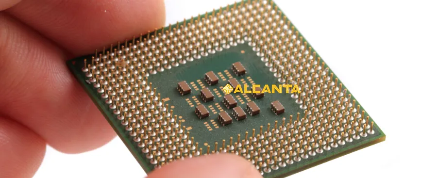
Ceramic QFN (Quad Flat No-leads) packages comprise several essential components, each playing a crucial role in the overall performance, reliability, and functionality of the package.
1. Semiconductor Chip:
At the heart of the Ceramic QFN Package lies the semiconductor chip, which contains the active electronic components responsible for performing specific functions, such as processing data, amplifying signals, or controlling power. The chip is typically mounted onto the ceramic substrate and wire bonded to connect its circuitry to the package’s external leads.
2. Ceramic Substrate:
The ceramic substrate serves as the foundation of the Ceramic QFN Package, providing mechanical support for the semiconductor chip and serving as a platform for interconnections. Ceramic materials offer excellent thermal conductivity, mechanical strength, and electrical insulation properties, making them ideal for applications requiring high-performance packaging solutions. The substrate also houses the solder pads and vias necessary for electrical connections and thermal management.
3. Solder Pad:
Solder pads are metalized areas on the bottom surface of the Ceramic QFN Package that facilitate the attachment of the package to the printed circuit board (PCB). During assembly, solder paste is applied to these pads, and the package is then placed onto the PCB and subjected to reflow soldering to create reliable electrical connections between the package and the PCB. Proper solder pad design and soldering techniques are critical for ensuring robust electrical and mechanical connections, as well as efficient heat dissipation.
4. Interconnects:
Interconnects refer to the conductive pathways that connect the semiconductor chip to the package’s external leads. These pathways can be implemented using wire bonding, flip-chip bonding, or other advanced interconnection technologies. The design and quality of interconnects significantly impact the electrical performance, signal integrity, and reliability of the Ceramic QFN Package. Proper alignment, bonding techniques, and material selection are essential for achieving optimal interconnect performance.
Importance of Each Component for Overall Performance:
– The semiconductor chip determines the functional capabilities and performance specifications of the Ceramic QFN Package, such as processing speed, power consumption, and signal processing capabilities.
– The ceramic substrate provides mechanical support, electrical insulation, and thermal management for the semiconductor chip, ensuring reliable operation in various environmental conditions and under different operating loads.
– Solder pads and interconnects play critical roles in establishing electrical connections between the package and the PCB, as well as facilitating efficient heat dissipation. Proper design and assembly techniques are essential to ensure robust electrical connections, thermal performance, and long-term reliability of the Ceramic QFN Package.
In summary, each component of the Ceramic QFN Package contributes to its overall performance, reliability, and functionality, making careful consideration of their design, materials, and assembly processes crucial for achieving optimal performance in electronic applications.
FAQs about ceramic qfn package
QFN packaging, short for Quad Flat No-leads, is a type of surface-mount semiconductor package that features a flat body with no leads extending from its edges. Instead, the electrical connections are made through exposed metal pads on the bottom surface of the package. QFN packaging is widely used in the electronics industry due to its compact size, excellent thermal performance, and simplified manufacturing process.
Some disadvantages of QFN packaging include soldering difficulties during assembly, challenges in repairing or reworking the package, potential reliability issues related to thermal cycling, and limitations in signal routing due to the absence of external leads.
There are various types of QFN packages, including:
Standard QFN: These are general-purpose QFN packages with a thin profile and low lead count, suitable for applications where space-saving and cost-effectiveness are essential.
Power QFN: Designed specifically for high-power applications, power QFN packages feature enhanced thermal management and robustness to handle higher current loads and dissipate heat more effectively.
Other specialized QFN variants may exist depending on specific application requirements, such as high-frequency QFNs or custom-designed QFN packages.
The components of a QFN package typically include:
Semiconductor Chip: The active electronic component responsible for performing specific functions.
Substrate: The foundation of the package, usually made of ceramic or organic material, providing mechanical support and serving as a platform for interconnections.
Solder Pads: Metalized areas on the bottom surface of the package for attaching to the printed circuit board (PCB) during assembly.
Interconnects: Conductive pathways connecting the semiconductor chip to the package’s external leads, facilitating electrical connections and signal transmission.

