
The Role of ABF Build Up Substrates in IC Packaging
In the rapidly evolving world of electronics, advanced semiconductor packaging has become crucial for meeting the performance demands of next-generation devices. As chip designs grow more complex and interconnect densities increase, traditional packaging technologies can no longer support the necessary electrical and thermal performance. This has led to the widespread adoption of ABF build up substrates, a revolutionary material technology developed by Ajinomoto. ABF, or Ajinomoto Build-up Film, serves as a key insulating layer in high-density interconnect (HDI) substrates used in packaging advanced chips. ABF build up substrates enable finer line spacing, improved signal integrity, and better thermal management, making them ideal for applications in high-performance computing (HPC), artificial intelligence (AI), and data centers. As the semiconductor industry pushes toward ever-smaller nodes and more powerful chipsets, ABF build up substrates have emerged as a critical enabler of innovation and efficiency in chip design and integration.
What Are ABF Build Up Substrates?
ABF build up substrates refer to a type of high-performance substrate material that uses Ajinomoto Build-up Film (ABF) as the dielectric layer in semiconductor packaging. Developed by the Japanese company Ajinomoto in the late 1990s, this material was originally created to meet the growing demands for miniaturization and high-speed signal transmission in integrated circuits. The ABF material is a photosensitive, epoxy-based resin that enables the formation of ultra-thin, high-resolution dielectric layers between copper traces, which is essential for advanced IC packages.
Advanced build-up substrates are now widely used in the packaging of cutting-edge semiconductor devices, including CPUs, GPUs, FPGAs, and ASICs—particularly those used in data centers, high-performance computing, and artificial intelligence (AI) systems. Compared to traditional PCB substrates, which rely on thicker and less precise insulating layers, these materials support finer line widths, tighter spacing, and greater layer counts. This enables much higher input/output (I/O) densities and better electrical performance, making them indispensable for next-generation chip designs.
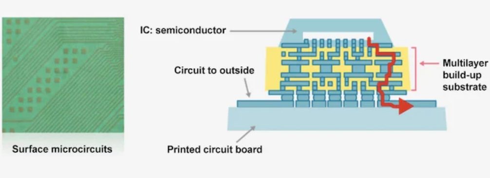
Structure and Function of ABF Build Up Substrates
ABF build up substrates are a specialized form of multilayer interconnect technology designed to meet the increasing performance requirements of modern semiconductor devices. The term “build-up” refers to the method of constructing additional dielectric and conductive layers on top of a central core substrate through a sequential lamination process. This approach allows manufacturers to achieve far greater interconnect density than with traditional substrate technologies.
The typical structure includes three main components: a rigid core layer (usually made of fiberglass-reinforced epoxy), one or more build-up dielectric layers made from Ajinomoto Build-up Film (ABF), and patterned copper layers that form the electrical traces. The ABF dielectric is essential for enabling fine-line patterning and precise layer stacking, both critical for supporting high-speed signal transmission and compact form factors.
A key feature of this substrate technology is the use of microvias—tiny vertical holes that connect one conductive layer to another. These microvias are typically formed using advanced laser drilling techniques that allow for extremely small and accurate via structures. This capability is crucial for fine-pitch interconnects required by advanced chips, such as CPUs and AI accelerators, enabling thousands of I/Os in a compact footprint.
Composition and Advantages of ABF Build Up Substrates
The superior performance of ABF build up substrates lies in the advanced chemical formulation of their dielectric layers. The core material used in these substrates is Ajinomoto Build-up Film (ABF), which is composed of a modified epoxy resin, specialized curing agents, and inorganic fillers. This carefully engineered combination provides a unique balance of electrical, thermal, and mechanical properties that are critical for advanced semiconductor packaging.
One of the most important attributes of ABF build up substrates is their excellent electrical insulation, which helps prevent signal cross-talk and power leakage in high-speed and high-density chip environments. Additionally, the material offers high thermal stability, ensuring reliability during chip operation and under harsh reflow soldering conditions. Another key advantage is its strong copper adhesion, which ensures the integrity of the conductive traces formed on each layer, supporting long-term package durability.
Another standout property of this material is its low dielectric constant, a crucial factor for maintaining signal integrity in high-frequency applications such as data processing and AI workloads. This makes it particularly well-suited for HDI (High-Density Interconnect) and UHDI (Ultra High-Density Interconnect) structures, where minimizing signal delay and maintaining precision routing are essential. These performance characteristics have made it the material of choice for high-end CPU, GPU, and AI chip packaging across the semiconductor industry.
Major Manufacturers of ABF Build Up Substrates
The production of ABF build up substrates involves a highly specialized and vertically integrated supply chain, with each stage requiring advanced materials and precise manufacturing techniques. At the foundation of this chain is Ajinomoto, the exclusive supplier of the Ajinomoto Build-up Film (ABF), Ajinomoto provides a proprietary material that enables high-density interconnects, and its consistent quality and performance make it indispensable for advanced substrate fabrication.
Once the ABF raw material is supplied, the next stage involves substrate manufacturers who use the film to produce high-performance build-up substrates. Leading players in this space include Ibiden and Shinko Electric Industries in Japan, Unimicron and Kinsus in Taiwan, as well as Nan Ya PCB and Taiwan Union Technology Corporation (TUC). Additionally, companies like ASE Group, one of the largest semiconductor packaging and testing houses, are also investing in substrate capabilities to support advanced IC packaging.
The overall supply chain for ABF build up substrates can be summarized as follows: Ajinomoto supplies the ABF film, which is then processed by substrate manufacturers into multilayer build-up substrates. These substrates are finally delivered to IC packaging houses, where they are integrated into advanced chip packages for products like CPUs, GPUs, FPGAs, and AI accelerators. This tightly coordinated chain is essential for meeting the performance and volume demands of today’s semiconductor industry.
ABF Build Up Substrates Supply Shortage
In recent years, the semiconductor industry has faced a significant supply shortage of ABF build up substrates, creating bottlenecks across the chip production ecosystem. This shortage has been driven by several compounding factors, each highlighting the critical role these substrates play in advanced electronics manufacturing.
One of the primary causes of the shortage is the soaring demand for high-end chips used in AI, 5G, and high-performance computing (HPC) applications. As devices become more powerful and compact, the need for complex packaging solutions has surged. However, producing these substrates is a highly complex and capital-intensive process, involving precise multilayer fabrication, microvia drilling, and strict quality control.
The number of qualified suppliers remains limited. Only a handful of companies, such as Ajinomoto (materials) and Unimicron or Ibiden (substrates), have the technological capabilities and production capacity to meet industry standards. Equipment bottlenecks and long lead times for capacity expansion have further restricted supply.
The market impact has been substantial. Major chipmakers like Intel and AMD have experienced packaging delays, affecting product launches and revenue projections. The shortage has also placed strain across the entire semiconductor supply chain, from foundries to system integrators.
To address this challenge, key players such as Ajinomoto and Unimicron are investing in capacity expansion, building new facilities and upgrading equipment. At the same time, R&D efforts are underway to explore alternative materials and technologies, such as SAP (semi-additive processing) and glass core substrates, which may eventually complement or replace ABF build up substrates in select applications. Nonetheless, ABF remains the gold standard for advanced packaging in the foreseeable future.
Future Trends in ABF Build Up Substrates Technology
As demand for higher performance and greater miniaturization accelerates across the semiconductor industry, ABF build up substrates are evolving rapidly to meet new technical and commercial challenges. Continued innovation in next-generation ABF materials is a major focus, with Ajinomoto and its partners developing improved resins with lower dielectric constants, enhanced thermal resistance, and better processability. These enhancements are crucial for supporting the ultra-fine line widths, thinner dielectrics, and increased layer counts needed in future high-performance packages.
At the same time, ABF build up substrates are being compared and contrasted with emerging packaging technologies, such as fan-out wafer-level packaging (FOWLP) and glass core substrates. While fan-out offers better form factor and thermal performance for some mobile and consumer applications, it still falls short in delivering the high I/O density and mechanical robustness required by high-end devices like CPUs, GPUs, and AI accelerators. Glass substrates are also gaining attention for their dimensional stability and potential in chiplet architectures, but they remain in early development stages with limited ecosystem support.
The market outlook from 2024 to 2028 points to strong and sustained growth for advanced packaging substrates, driven by advancements in AI, cloud computing, autonomous vehicles, and 5G infrastructure. As chip complexity increases and packaging becomes more central to overall performance, the role of ABF build up substrates will become even more critical. Investments in R&D, supply chain capacity, and alternative hybrid substrate designs will shape the next phase of this essential technology’s evolution.
FQAs Abut ABF Build Up Substrates
What are ABF substrates?
Film (ABF) as the insulating dielectric layer. They are used in high-density interconnect (HDI) substrates to support the packaging of advanced semiconductor chips such as CPUs, GPUs, FPGAs, and ASICs. ABF substrates enable fine line widths, high I/O density, and reliable signal integrity, making them ideal for high-performance computing and AI applications.
Is there a shortage of ABF substrate?
Yes, there has been a shortage of ABF substrates in recent years. The main causes include skyrocketing demand for high-end chips (AI, 5G, HPC), the complex and capital-intensive nature of manufacturing ABF substrates, and a limited number of qualified suppliers. This has impacted chip production timelines for major semiconductor companies like Intel and AMD.
What is a buildup substrate?
A buildup substrate is a type of multilayer circuit board where additional layers are constructed on a core layer through sequential lamination. These added layers use insulating materials like ABF and feature microvias and thin copper lines to support dense interconnects. Buildup substrates are essential for modern IC packaging, especially in high-density or ultra-high-density designs.
What is the composition of ABF material?
ABF material consists of a modified epoxy resin, specialized curing agents, and inorganic fillers. This formulation provides key properties such as:
-
Excellent electrical insulation
-
High thermal stability
-
Strong copper adhesion
-
Low dielectric constant, which supports high-speed signal transmission
These characteristics make it suitable for advanced HDI and UHDI packaging applications.

