
What is ABF Substrate? Key to Semiconductor Advancements
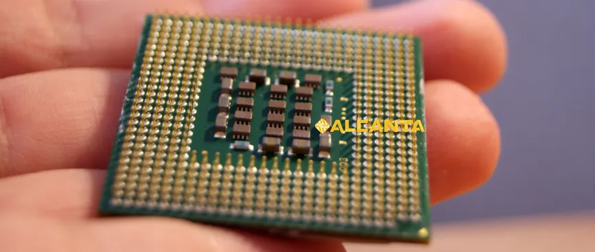
What is ABF substrate? ABF substrate, short for Ajinomoto Build-Up Film substrate, is a crucial component in the semiconductor industry. Essentially, ABF substrate refers to a specialized material utilized in semiconductor packaging and interconnection processes. Its significance lies in its ability to provide high-density interconnects, enabling efficient communication between semiconductor components. ABF substrate plays a pivotal role in the development of advanced electronic devices, such as microprocessors and memory chips. Its unique properties make it suitable for various applications, including flip-chip packaging, multi-chip modules, and high-speed data transmission systems. Understanding what ABF substrate is and its applications is essential for grasping the complexities of modern semiconductor technology.
What is ABF Substrate?
ABF stands for Ajinomoto Build-up Film, a proprietary dielectric material developed by Ajinomoto Fine-Techno.
It’s an epoxy-based resin film containing inorganic fillers and curing agents, designed for multilayer buildup substrates used in high-density packages.
Unlike traditional PCB laminates, ABF films enable ultra-fine circuit patterning — down to 2/2 µm line/space — and excellent electrical insulation, low dielectric loss, and dimensional stability.
Typical ABF film properties:
-
Dielectric constant (Dk): 3.0–3.3
-
Glass transition temperature (Tg): 230–250 °C
-
Coefficient of thermal expansion (CTE): ~55 ppm/°C
-
Compatible with laser-drilled microvias (down to 10 µm)
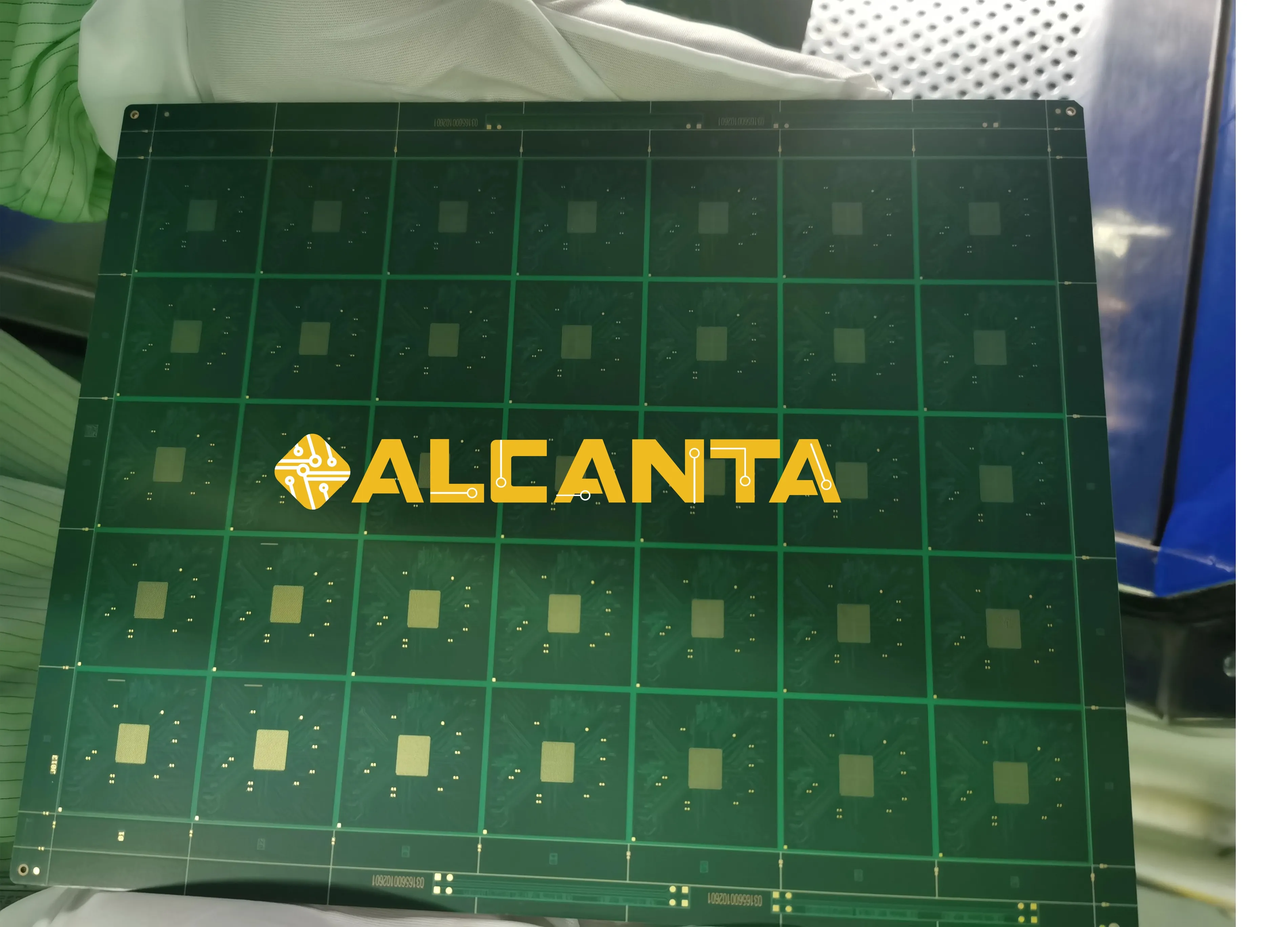
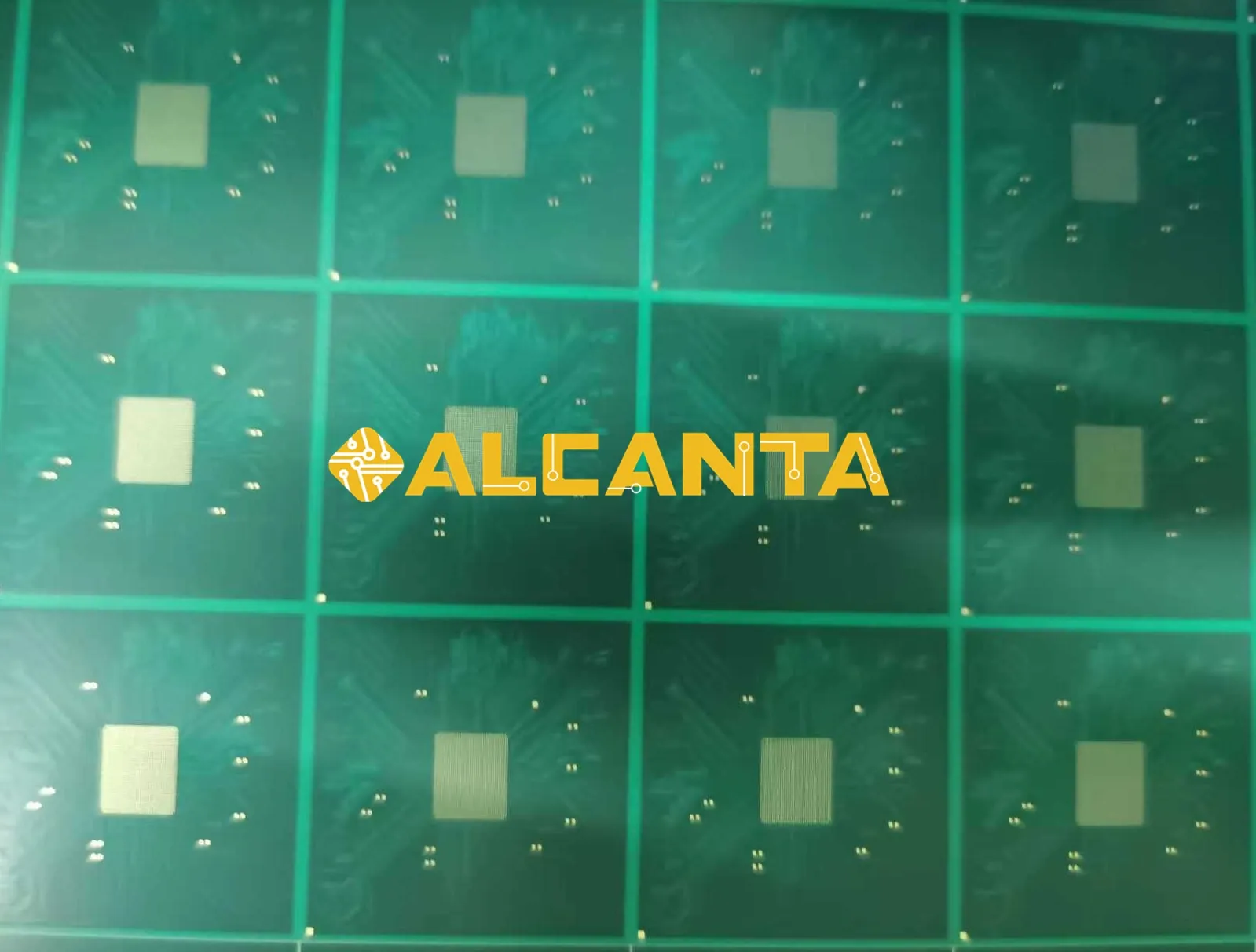
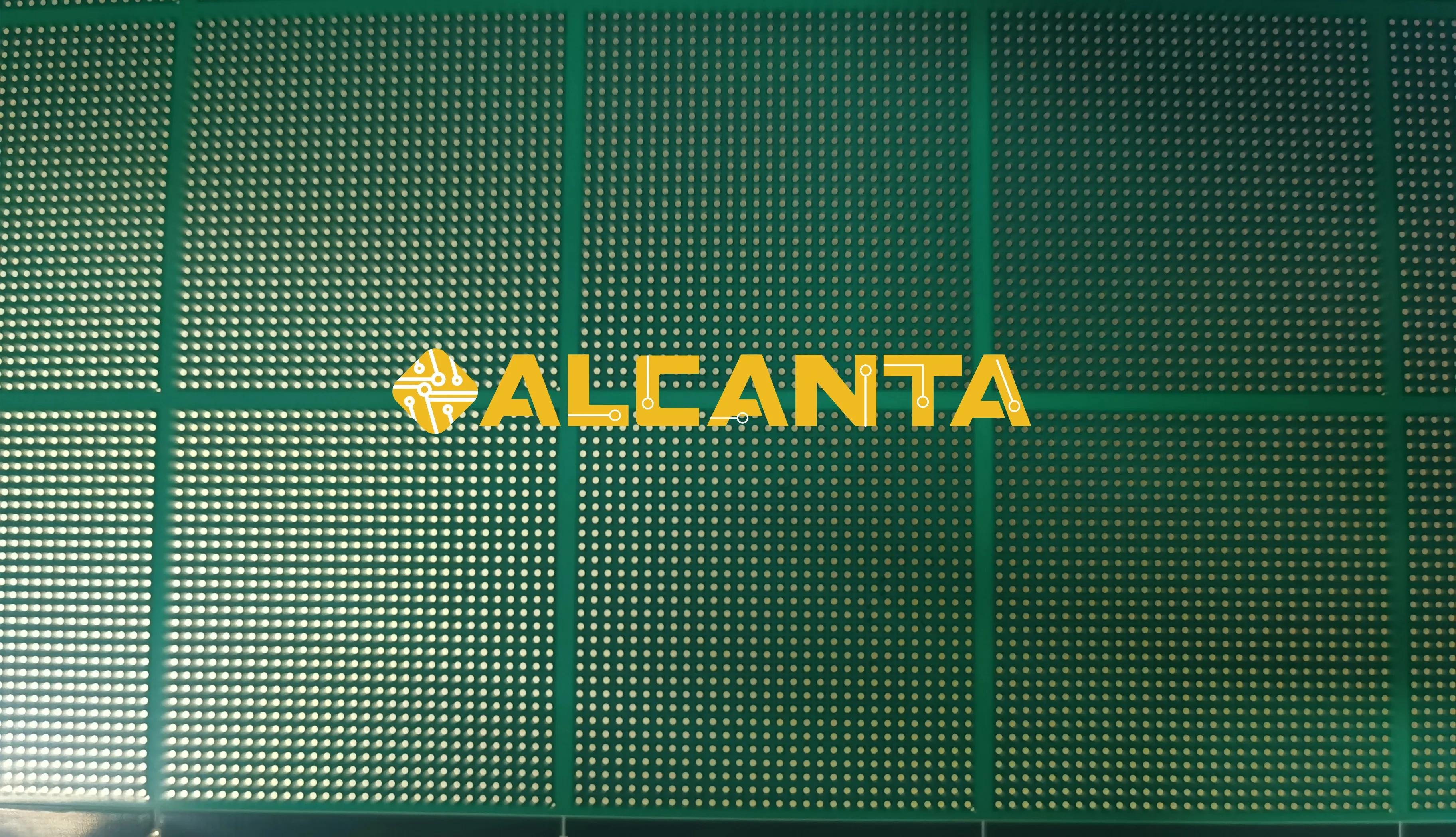
In a build-up substrate, ABF layers are stacked over a copper-clad core, alternating with fine copper circuits — forming a multilayer interconnect structure between silicon die and the PCB.
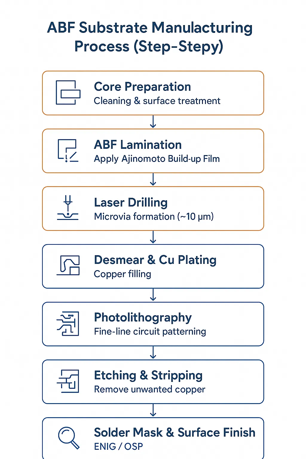
ABF Substrate Manufacturing Process (Step-by-Step)
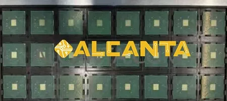
The manufacturing of ABF substrates is a multi-stage process that blends microfabrication, lamination, laser drilling, and electroplating technologies — all executed in a highly controlled cleanroom environment.
Below is a detailed look at each step:
Step 1: Core Preparation
The process begins with a copper-clad core (BT or modified epoxy).
It’s cleaned, micro-etched, and surface-treated for adhesion.
➡ Goal: Ensure flatness (<0.2%) and clean bonding surface.
Step 2: ABF Lamination
Ajinomoto Build-up Film (ABF) is laminated under heat and pressure onto the core.
Typical ABF layer thickness: 10–15 µm.
➡ Goal: Create a smooth, thin dielectric ready for microvia formation.
Step 3: Laser Drilling
UV lasers form microvias (~10 µm) connecting build-up layers.
Position accuracy: ±3 µm.
➡ Goal: Establish fine-pitch interconnects between copper layers.
Step 4: Desmear & Copper Plating
Residual debris is removed via plasma or chemical desmear.
Then, copper is plated to fill vias and form a conductive layer.
➡ Goal: Build strong via connections and prepare for patterning.
Step 5: Photolithography
Photoresist is applied, exposed, and developed to define fine-line circuits.
ABF supports 2/2 µm line/space capability.
➡ Goal: Pattern ultra-fine wiring for high-speed signal routing.
Step 6: Etching & Stripping
Unwanted copper is etched away to form the final traces.
➡ Goal: Achieve clean, precise circuit definition.
Step 7: Solder Mask & Surface Finish
Solder mask coating, exposure, and curing are followed by surface finishes such as ENIG or OSP.
➡ Goal: Protect copper, enhance solderability, and prevent oxidation.
Step 8: Final Inspection & Testing
Electrical testing (flying probe), AOI, impedance checks, and reliability qualification ensure 100% yield traceability.
Key Process Control Parameters
| Process Step | Key Parameters | Control Method |
|---|---|---|
| Lamination | 120–180 °C, 0.2–1 MPa | Temp/pressure log |
| Laser via | 10 µm ±2 µm | Optical inspection |
| Copper plating | Thickness 5–10 µm | Cross-section SEM |
| Photolithography | 2/2 µm line/space | CD-SEM / AOI |
| Surface finish | ENIG 0.05–0.2 µm Au | XRF |
Key Technical Considerations in ABF Substrate Design
This section outlines the critical factors to consider when designing ABF substrates, ensuring optimal performance and reliability in semiconductor applications.
Coefficient of Thermal Expansion (CTE) Matching
CTE matching is essential to ensure compatibility between the substrate and the semiconductor chip, particularly under varying thermal conditions.
Material Engineering: Resin formulations and filler materials are carefully selected to achieve low and stable CTE values, ensuring dimensional stability and thermal reliability.
Compatibility with Chip Materials: The ABF substrate must closely align its CTE with the silicon die to minimize mechanical stress during thermal cycling. Disparities in expansion rates can lead to delamination, cracking, or solder joint failure.
High-Density I/O Requirements
Modern semiconductor devices demand substrates that support high input/output (I/O) densities, driving the need for advanced design solutions.
Interlayer Connection Optimization: The size, distribution, and reliability of microvias are critical for achieving efficient electrical interconnections between layers. Designers must consider via-in-pad designs and stacked via configurations to support high I/O densities without compromising mechanical integrity.
Miniaturization Challenges: As chip designs continue to shrink, ABF substrates must accommodate increased pin counts and complex signal routing within limited space. This necessitates advanced photolithography and precision laser drilling technologies to produce microvias and fine line/spacing patterns.
Signal Integrity and Power Distribution Network (PDN)
Maintaining signal integrity and an efficient PDN are critical for ensuring high performance and minimizing electromagnetic interference (EMI).
Low-Impedance Design: PDN optimization focuses on creating uniform power and ground planes to minimize impedance. This ensures stable power delivery and reduces voltage fluctuations, crucial for high-speed signal transmission.
Signal Integrity Analysis: Techniques such as impedance matching, controlled dielectric properties, and the use of low-loss materials help reduce crosstalk, signal reflection, and attenuation.
Thermal Management and Reliability
Efficient thermal management and long-term reliability are vital for ABF substrates, especially in high-performance and high-power applications.
Long-Term Reliability Testing: ABF substrates undergo rigorous testing to validate their resistance to moisture, aging, and thermal stress. Key metrics include warpage control, delamination resistance, and solder joint durability under prolonged operational conditions.
Selection of Thermal Interface Materials: Integrating materials with high thermal conductivity, such as metal layers or specialized fillers, ensures effective heat dissipation and stability during operation.
Get a abf substrateQuick Quote
ABF Substrate Assembly Process Issues
The assembly of ABF (Ajinomoto Build-Up Film) substrates involves high precision and multiple advanced processes. Below are the main technical challenges engineers face during ABF substrate assembly.
Microvia Formation
Microvias enable high-density interconnects, but laser drilling precision is critical.
-
Misalignment or incomplete vias cause open circuits or poor signal paths.
-
Solution: Use calibrated laser systems and inline AOI to ensure consistent via quality.
Thermal Stress & Reflow Control
During solder reflow, ABF layers can warp or delaminate under uneven heating.
-
Excessive heat can damage dielectric layers or affect copper adhesion.
-
Solution: Optimize reflow profiles and use step-cooling to control temperature gradients.
Alignment & Registration
Fine-pitch multi-layer structures require micron-level alignment.
-
Poor layer registration leads to shorts or open circuits.
-
Solution: Automated optical alignment and laser-guided bonding improve accuracy.
Soldering Reliability
Dense I/O designs make solder joint quality a critical factor.
-
Risks include bridging, voiding, or cold joints.
-
Solution: Use fine-pitch solder pastes, nitrogen reflow, and controlled flux chemistry.
Warpage & Mechanical Stress
Thin ABF cores can warp during lamination or reflow.
-
Warpage affects component coplanarity and yield.
-
Solution: Balance CTE across layers and use symmetrical stack-up design.
Surface Finish & Solderability
Surface treatment impacts wetting and long-term reliability.
-
Poor finish causes weak solder joints or oxidation.
-
Solution: Apply ENIG or OSP finishes and ensure pre-assembly cleaning.
High-Density Component Integration
Fine-pitch and microbump packaging challenge assembly precision.
-
Misplaced bumps or short circuits reduce yield.
-
Solution: Use advanced flip-chip bonding tools with precise placement control.
Get a what is abf substrate Quick Quote
ABF vs BT Substrate: Material and Performance Comparison
Both ABF (Ajinomoto Build-up Film) and BT (Bismaleimide Triazine) are used in package substrates, but their roles differ sharply.
| Property | ABF Substrate | BT Substrate |
|---|---|---|
| Dielectric constant (Dk) | 3.0–3.3 | 3.8–4.2 |
| Glass transition temperature (Tg) | ≥230 °C | 180–200 °C |
| CTE (ppm/°C) | ~50–60 | ~70–80 |
| Line/space capability | 2/2 µm | 10/10 µm |
| Microvia size | <10 µm | >50 µm |
| Applications | HPC, GPU, AI processors | Memory, consumer ICs |
Applications of ABF Substrates
ABF substrates are essential for:
-
High-performance CPUs and GPUs (Intel, NVIDIA, AMD)
-
AI and Data Center accelerators
-
Networking ASICs and 5G processors
-
2.5D interposers and advanced SiP modules
With increasing demand for AI and HPC packaging, the need for ultra-fine ABF substrates continues to surge — driving material innovation (e.g., lower Dk ABF, glass core integration).
FAQs About What is ABF substrate
What is an ABF substrate?
ABF (Ajinomoto Build-Up Film) substrate is a high-density interposer used in advanced semiconductor packaging. It consists of multiple layers of polymer films and copper, enabling fine-line routing for CPUs, GPUs, and SoCs.
How is an ABF substrate different from a traditional BT substrate?
ABF substrates allow finer line/space (L/S) down to 30 µm, support higher I/O counts, and exhibit better thermal expansion matching with silicon, improving signal integrity in high-speed applications.
What are the main materials used in ABF substrates?
Core materials include photoimageable ABF films, copper foil for signal and power layers, and dielectric prepregs. ABF films act as insulating build-up layers that are patterned by photolithography.
What is the standard manufacturing process for ABF substrates?
The process includes lamination of ABF films and copper, laser drilling of microvias, sequential build-up of signal and power layers, copper plating, and precision patterning to create multilayer interconnects.
What are microvias, and why are they critical in ABF substrates?
Microvias are tiny vertical interconnects that connect layers in the substrate. They enable high-density routing, minimize signal loss, and are essential for fine-pitch high-speed packages.
How does ABF substrate improve signal integrity?
ABF’s low dielectric constant and precise layer alignment reduce crosstalk, maintain impedance control, and ensure minimal propagation delay, which is crucial for high-frequency processor signals.
What challenges do engineers face during ABF substrate assembly?
Challenges include microvia filling, delamination risk, substrate warpage, and copper trace reliability during high-temperature soldering. Tight process control and defect monitoring are essential.
Which applications rely most on ABF substrates?
High-performance CPUs, GPUs, FPGAs, and AI accelerators use ABF substrates due to their fine-pitch capability, high I/O density, and excellent thermal and electrical performance.
How does ABF substrate compare to leadframe packaging?
ABF supports multi-layer interconnects, ultra-fine pitch, and higher I/O density, whereas leadframes are simpler, cheaper, and better suited for low-to-mid-range power ICs but limited for high-speed or high-density packages.
Can ABF substrates meet next-generation chip requirements?
Yes. ABF substrates support sub-5 nm node scaling, advanced high-frequency signaling, and high thermal reliability, making them suitable for future AI, HPC, and mobile SoC applications.

