
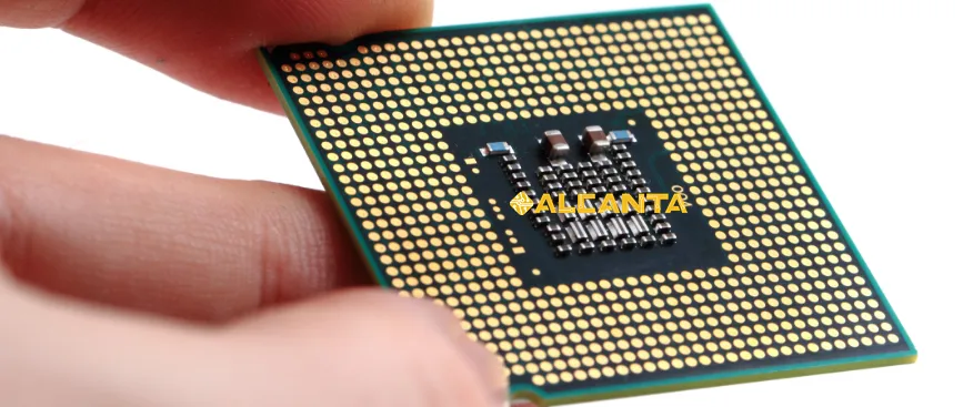
Reliable Performance: 4-Layer PCB Testing
Printed Circuit Boards (PCBs) serve as the backbone of modern electronic devices, facilitating the interconnection of components through conductive pathways. The fabrication and assembly process involves intricate stages of designing, etching, and soldering, ensuring precise execution to meet functional requirements. However, even with meticulous manufacturing, defects may occur, underscoring the critical role of electrical testing. Electrical testing serves as the final checkpoint, verifying the integrity and functionality of PCBs before deployment. Among various PCB configurations, 4-layer PCB substrates stand out for their versatility, accommodating complex circuitry while maintaining compact form factors. Understanding their significance is crucial, as they underpin the performance of diverse electronic applications, from consumer electronics to aerospace systems.
Understanding PCB Electrical Testing
PCB electrical testing is a pivotal phase in the quality assurance process, encompassing a range of assessments to validate the integrity and functionality of the board. At its core, electrical testing evaluates the connectivity, insulation, and performance of the circuitry.
Explanation of PCB Electrical Testing:
This process involves subjecting the PCB to a battery of tests to ensure it meets design specifications and operational requirements. It includes both automated and manual examinations, examining various electrical parameters to detect potential faults or deviations.
Types of Electrical Tests:
1. Continuity Testing: Ensures the continuity of conductive pathways, identifying any breaks or discontinuities in the circuit.
2. Insulation Resistance Testing: Measures the resistance between conductive elements and insulating materials, identifying potential short circuits or insulation failures.
3. Impedance Testing: Assesses the impedance characteristics of signal traces, critical for maintaining signal integrity and minimizing transmission losses.
4. Capacitance Testing: Evaluates the capacitance between adjacent traces or components, ensuring proper functionality and signal isolation.
5. Functional Testing: Validates the overall functionality of the PCB by simulating real-world operating conditions and assessing performance against predefined criteria.
Importance of Thorough Electrical Testing:
Thorough electrical testing is indispensable for identifying defects that may compromise the performance or reliability of the PCB. By detecting faults early in the manufacturing process, it mitigates the risk of costly rework or product recalls, ensuring compliance with quality standards and customer expectations. Moreover, it instills confidence in the reliability of the final product, crucial for applications where downtime or failure is not an option, such as aerospace, medical, or automotive electronics. Ultimately, rigorous electrical testing safeguards against potential failures, enhancing the overall quality and longevity of electronic devices.
Tracing a 4-Layer PCB
Overview of the Layers:
A 4-layer PCB consists of four layers of conductive material separated by insulating layers, offering enhanced flexibility and complexity compared to single or double-layer boards. The layers typically include:
1. Top Layer (Signal Layer): Houses the primary signal traces and components, facilitating interconnection between components.
2. Inner Signal Layers: Additional layers sandwiched between the outer layers, providing space for routing complex signal paths and reducing electromagnetic interference (EMI).
3. Ground Plane: One of the inner layers dedicated to grounding, ensuring stable reference potential for signal integrity and noise reduction.
4. Power Plane: The other inner layer dedicated to power distribution, supplying voltage to components and minimizing voltage drops.
Techniques for Tracing Signal Paths:
Tracing signal paths through the layers of a 4-layer PCB requires careful consideration and specialized techniques:
1. Schematic Analysis: Begin by examining the schematic diagram to understand the connectivity between components and identify critical signal paths.
2. Layer Stackup Analysis: Understand the layer stackup configuration to determine the signal routing strategy and optimize signal integrity.
3. Cross-Sectional Analysis: Utilize cross-sectional views to visualize the signal traces as they traverse through different layers, ensuring proper routing and avoiding signal interference.
4. PCB Design Tools: Employ advanced PCB design software with layer visualization features to trace signal paths accurately and efficiently.
Importance of Accurate Tracing:
Accurate tracing of signal paths is paramount for effective troubleshooting and debugging of PCBs:
1. Fault Identification: Precise tracing helps pinpoint potential faults or signal integrity issues, enabling swift diagnosis and resolution of problems.
2. Signal Integrity: Properly traced signal paths minimize signal distortion, reflection, and crosstalk, ensuring reliable communication between components.
3. EMI Reduction: Well-routed signal paths help mitigate electromagnetic interference, enhancing the overall performance and reliability of the PCB.
4. Efficient Debugging: Accurate tracing streamlines the debugging process, reducing downtime and costs associated with rework or product recalls.
In essence, accurate tracing of signal paths is indispensable for optimizing PCB performance, ensuring functionality, and meeting quality standards.
Rules for Designing a 4-Layer PCB
Overview of Design Considerations:
Designing a 4-layer PCB requires careful attention to various factors to ensure optimal performance and manufacturability:
1. Layer Stackup: Determine the layer stackup configuration, considering signal integrity, power distribution, and EMI shielding.
2. Component Placement: Strategically place components to minimize signal path lengths, reduce noise coupling, and optimize thermal management.
3. Routing Strategy: Develop a routing strategy that balances signal integrity, EMI mitigation, and manufacturability, considering high-speed signals, impedance control, and differential pairs.
4. Power Distribution: Design robust power distribution networks, including power planes and decoupling capacitors, to minimize voltage drops and ensure stable power delivery.
5. Signal Integrity: Address signal integrity issues such as impedance matching, signal reflections, and crosstalk through proper termination, controlled impedance routing, and signal isolation techniques.
Guidelines for Layout, Routing, and Signal Integrity:
1. Signal Layer Allocation: Distribute critical signals across different layers to minimize interference and optimize signal integrity.
2. Routing Density: Maintain appropriate routing density to avoid signal congestion and ensure manufacturability, considering signal layers’ capabilities.
3. Via Placement: Place vias strategically to minimize signal distortion and impedance discontinuity, considering signal layers’ proximity and impedance requirements.
4. Ground Plane Design: Ensure a continuous and low-impedance ground plane to provide a stable reference for signal return paths and mitigate EMI.
5. Impedance Control: Implement controlled impedance routing for high-speed signals to maintain signal integrity and prevent signal degradation.
6. Differential Pair Routing: Route differential pairs with matched lengths and spacing, using differential pair routing techniques to minimize skew and ensure signal integrity.
Importance of Adhering to Design Rules:
Adhering to design rules is crucial for achieving optimal performance and manufacturability of 4-layer PCBs:
1. Performance Optimization: Following design rules ensures signal integrity, reduces EMI, and enhances the overall performance of the PCB.
2. Manufacturability: Design rules facilitate efficient manufacturing processes, reducing the risk of fabrication errors, assembly issues, and rework.
3. Cost Efficiency: By optimizing performance and manufacturability, adherence to design rules minimizes production costs and time-to-market, enhancing the PCB’s competitiveness in the market.
In conclusion, meticulous adherence to design considerations and guidelines is essential for designing high-quality 4-layer PCBs that meet performance requirements, ensure manufacturability, and minimize production costs.
Parameters of PCB Electrical Testing
Detailed Explanation of Parameters:
During PCB electrical testing, several key parameters are measured to assess the board’s quality and functionality:
1. Continuity: Checks for uninterrupted flow of current through conductive pathways, ensuring that all connections are intact and there are no open circuits.
2. Insulation Resistance: Measures the resistance between conductive elements and insulating materials, verifying that there are no short circuits or leakage paths that could compromise safety or functionality.
3. Capacitance: Evaluates the capacitance between conductive elements, ensuring proper electrical isolation and signal integrity, particularly in high-frequency circuits.
4. Impedance: Determines the opposition to the flow of alternating current, crucial for maintaining signal integrity, minimizing reflections, and ensuring proper transmission of high-speed signals.
Key Metrics and Importance:
1. Continuity:
– Importance: Ensures that all connections are intact, preventing signal loss or malfunction due to open circuits.
– Impact on Quality: Lack of continuity can lead to non-functional circuits or unreliable operation, affecting the overall quality and reliability of the PCB.
2. Insulation Resistance:
– Importance: Prevents short circuits and electrical leakage, ensuring safety and reliability in operation.
– Impact on Quality: Poor insulation resistance can result in electrical faults, overheating, or damage to components, compromising the PCB’s reliability and safety.
3. Capacitance:
– Importance: Maintains signal integrity by minimizing noise and interference, particularly in high-frequency circuits.
– Impact on Quality: Inaccurate capacitance values can lead to signal distortion, degraded performance, or susceptibility to electromagnetic interference (EMI), affecting the PCB’s functionality and reliability.
4. Impedance:
– Importance: Ensures proper transmission of high-speed signals, minimizing signal distortion and reflections.
– Impact on Quality: Deviations in impedance can cause signal degradation, timing errors, or signal integrity issues, impacting the PCB’s performance and reliability, especially in high-speed or high-frequency applications.
Assessing PCB Quality and Reliability:
Each parameter plays a critical role in assessing PCB quality and reliability:
– Continuity ensures proper functionality and prevents circuit failures.
– Insulation resistance ensures safety and prevents electrical faults.
– Capacitance and impedance contribute to signal integrity, minimizing noise and ensuring reliable communication.
Overall, thorough evaluation of these parameters during PCB electrical testing is essential for ensuring the quality, reliability, and performance of electronic devices.
Parameters of PCB Electrical Testing
Detailed Explanation of Parameters:
1. Continuity:
– Continuity testing verifies if there’s a complete path for electrical current flow between two points on the PCB. It’s usually performed using a multimeter to check for resistance or conductivity.
2. Insulation Resistance:
– Insulation resistance measures the resistance between conductive elements and insulating materials. It ensures there are no unintended connections or leakage paths, maintaining electrical isolation and safety.
3. Capacitance:
– Capacitance testing determines the ability of the PCB to store electrical charge between conductive elements. It’s crucial for maintaining signal integrity, especially in high-frequency circuits, by reducing noise and interference.
4. Impedance:
– Impedance measures the opposition to the flow of alternating current in a circuit. It’s critical for high-speed signal transmission, ensuring minimal distortion and reflections, and maintaining signal integrity.
Key Metrics and Importance:
1. Continuity:
– Importance: Continuity ensures that all required connections are intact, preventing open circuits that could lead to malfunction or failure.
– Impact on Quality: Lack of continuity can result in non-functional circuits or unreliable operation, significantly impacting PCB quality and reliability.
2. Insulation Resistance:
– Importance: Insulation resistance prevents unintended electrical connections or leakage paths, ensuring safety and reliability in operation.
– Impact on Quality: Poor insulation resistance can lead to electrical faults, short circuits, or damage to components, compromising the PCB’s reliability and safety.
3. Capacitance:
– Importance: Capacitance helps maintain signal integrity by reducing noise and interference, particularly in high-frequency circuits.
– Impact on Quality: Inaccurate capacitance values can lead to signal distortion, degraded performance, or susceptibility to electromagnetic interference (EMI), affecting the PCB’s functionality and reliability.
4. Impedance:
– Importance: Impedance ensures proper transmission of high-speed signals, minimizing distortion and reflections.
– Impact on Quality: Deviations in impedance can cause signal degradation, timing errors, or signal integrity issues, impacting the PCB’s performance and reliability, especially in high-speed or high-frequency applications.
Assessing PCB Quality and Reliability:
Each parameter is crucial for assessing different aspects of PCB quality and reliability:
– Continuity ensures proper functionality and prevents circuit failures.
– Insulation resistance ensures safety and prevents electrical faults.
– Capacitance and impedance contribute to signal integrity, ensuring reliable communication and minimizing noise.
Overall, evaluating these parameters during PCB electrical testing is essential for ensuring high-quality, reliable PCBs that meet performance requirements and safety standards.
Product Spotlight: 4-Layer PCB Substrate Electrical Testing
Introduction to ACI PCB’s Capabilities:
ACI PCB stands at the forefront of 4-layer PCB fabrication and assembly, offering cutting-edge solutions tailored to meet diverse industry needs. With years of experience and expertise, ACI PCB specializes in delivering high-quality, reliable 4-layer PCBs that exceed customer expectations.
Highlighting ACI PCB’s Expertise:
ACI PCB is renowned for its unparalleled expertise in electrical testing and quality assurance. Utilizing state-of-the-art equipment and advanced testing methodologies, ACI PCB ensures that every 4-layer PCB undergoes rigorous testing to guarantee optimal performance and reliability. From continuity and insulation resistance to impedance and capacitance, ACI PCB leaves no stone unturned in verifying the integrity and functionality of each PCB.
Case Studies and Examples:
1. Consumer Electronics Application: ACI PCB partnered with a leading consumer electronics company to manufacture 4-layer PCBs for their latest smart home device. Through comprehensive electrical testing, ACI PCB identified and rectified potential signal integrity issues, ensuring flawless performance and reliability of the final product.
2. Medical Device Development: ACI PCB collaborated with a medical device manufacturer to produce 4-layer PCBs for a critical patient monitoring system. By meticulously testing each PCB for insulation resistance and capacitance, ACI PCB ensured compliance with stringent safety standards, guaranteeing the utmost reliability in healthcare settings.
3. Automotive Electronics Integration: ACI PCB supported an automotive electronics supplier in developing 4-layer PCBs for advanced vehicle navigation systems. Leveraging sophisticated impedance testing techniques, ACI PCB optimized signal transmission, minimizing noise and ensuring seamless integration into the vehicle’s electronics ecosystem.
In each of these cases, ACI PCB’s dedication to electrical testing and quality assurance played a pivotal role in delivering superior 4-layer PCBs that met the highest standards of performance, reliability, and safety. With ACI PCB as a trusted partner, customers can confidently rely on their 4-layer PCB solutions for a wide range of applications across industries.
FAQs about 4 layer pcb substrate electrical test
PCBs are electrically tested using various methods and equipment. These tests typically include continuity testing to check for open or short circuits, insulation resistance testing to ensure proper isolation between conductive elements, impedance testing to verify signal integrity, and functional testing to assess overall performance.
Tracing a 4-layer PCB involves understanding the layer stackup and utilizing specialized techniques. This includes analyzing the schematic diagram to identify signal paths, utilizing PCB design software to visualize traces through different layers, and employing cross-sectional analysis to ensure proper routing and signal integrity.
Rules for 4-layer PCB design include considerations such as layer stackup configuration, component placement, routing strategy, power distribution, signal integrity, impedance control, and ground plane design. Adhering to these rules ensures optimal performance, manufacturability, and reliability of the PCB.
Parameters of PCB electrical testing include continuity, insulation resistance, capacitance, and impedance. Continuity testing verifies the flow of current through conductive pathways, insulation resistance testing measures resistance between conductive and insulating materials, capacitance testing evaluates charge storage between conductive elements, and impedance testing measures opposition to alternating current flow for signal transmission. These parameters are critical for assessing PCB quality and reliability.

