① Needs Analysis
Conduct a thorough analysis of customer requirements and technical specifications in initial communications to accurately capture the customized Package Substrate/HDI PCB requirements.


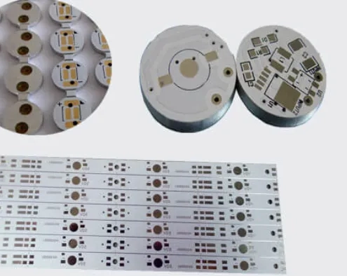
ALCANTA PCB specializes in manufacturing various types of packaging substrates, ranging from 2 layers to 26 layers. We support a minimum trace/spacing of 9μm and a minimum laser via hole size of 55μm. Our company uses industry-leading packaging substrate materials, with most of them sourced from Japan, such as Mitsubishi’s BT series (e.g., L-832NX, HL832NX), Showa Denko materials (e.g., MCL-E705G, MCL-E-770G, MCL-E-700G, MCL-E-795G), and Ajinomoto materials (e.g., GX92R, GXT31R2, GZ41R2H, GL102R8HF, GL103R8H). Additionally, we produce high-precision HDI PCBs with trace/spacing as small as 15μm. We also offer glass-core FCBGA substrates ranging from 4 layers to 20 layers, which deliver superior flatness. Furthermore, we have a wide variety of materials not listed here, and we welcome you to share your specific requirements so we can customize production accordingly.


We produce BGA substrates, FCBGA substrates, Glass substrates,FCCSP substrates and other types package substrates with ultra-small trace and pitch, we have various types of materials, the substrates will be produced in a factory of 20,000 employees, So,the quality is perfect, the delivery time is fast, the price is reasonable.

SIP Package, which encompasses various advanced packaging technologies such as Wire Bonding & Die Stack, Flip Chip, Embedded, Package on Package, Multi-chip Module, Package in Package, and other innovative solutions, offers a range of options for optimizing performance and space utilization in electronic devices.

When you design the package substrate, if you have any design questions, such as: standard laser via hole diameter(4mil), the minimum via hole diameter(2.2mil), and the minimum marks, spacing, solder resistance design, material selection, etc., or production process capability details, you can contact us at any time, it is our pleasure to help you.
Conduct a thorough analysis of customer requirements and technical specifications in initial communications to accurately capture the customized Package Substrate/HDI PCB requirements.
Please send your Package Substrate gerber files or PCB gerber files, Each BGA Substrate/PCB are individually customized, so we have to confirm all the details, whether it can meet customer requirements, we will strictly according to customer requirements production. after checking, if not big problem, we will send price and lead time back to you.
After you agree the price and lead time, please send a PO list at first, then, help to do the payment, Our engineers will confirm all the details again, and the EQ confirmation document will be sent to you. All the questions have been confirmed clearly, and the production has been carried out according to the customer’s requirements.
After we finsihed all EQ(design detail) list checking, our engineer will make the working gerber files, if you need, the working gerber files will be sent to you, your engineer need to compare it , if no other questions, you need to approve to produce the Packaging Substrates or HDI PCBs.
When we finished the Package Substrates or HDI PCBs, All the substrates and pcb boards will be 100% passed the electric test, So, There won’t be any open circuit, short circuit problems.
We mainly use the official DHL, Fedex air freight to send goods to customers, fast, efficient and safe. If the customer has other shipping requirements, we will send the goods to the designated place according to the customer’s requirements.


Specializes in research, development, production, and sales of a wide range of PCB types across various industries. Our offerings include HDI, multilayer, rigid-flex, heavy copper, metal-based, high-frequency, and flex boards. These products serve industrial control, medical electronics, automotive electronics, telecommunications, LED lighting, and other sectors. With a focus on innovation and expanding product applications, we excel in the low-volume market segment. Our capabilities include customized PCB production tailored to customer specifications, leveraging Advanced MSAP and SAP technologies. We specialize in FC BGA Packaging Substrates ranging from 4 to 16 layers, achieving industry-leading smallest gap and trace dimensions of 9um/9um, utilizing ABF base materials.
 https://pcbmake.com/wp-content/uploads/2025/09/copper-core-pcb.webp
394
711
pcbmake_admin
http://pcbmake.com/wp-content/uploads/2024/02/A去水印-1030x138.png
pcbmake_admin2025-09-18 07:13:482025-09-18 07:13:48Copper Core PCB vs Aluminium Core PCB Explained
https://pcbmake.com/wp-content/uploads/2025/09/copper-core-pcb.webp
394
711
pcbmake_admin
http://pcbmake.com/wp-content/uploads/2024/02/A去水印-1030x138.png
pcbmake_admin2025-09-18 07:13:482025-09-18 07:13:48Copper Core PCB vs Aluminium Core PCB Explained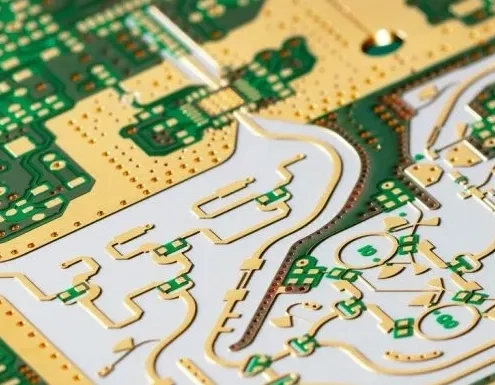 https://pcbmake.com/wp-content/uploads/2025/09/microwave-PCB-Manufacturer-1.webp
385
784
pcbmake_admin
http://pcbmake.com/wp-content/uploads/2024/02/A去水印-1030x138.png
pcbmake_admin2025-09-16 07:58:502025-09-18 06:55:23Microwave PCB Manufacturers | RF Design and Fabrication
https://pcbmake.com/wp-content/uploads/2025/09/microwave-PCB-Manufacturer-1.webp
385
784
pcbmake_admin
http://pcbmake.com/wp-content/uploads/2024/02/A去水印-1030x138.png
pcbmake_admin2025-09-16 07:58:502025-09-18 06:55:23Microwave PCB Manufacturers | RF Design and Fabrication https://pcbmake.com/wp-content/uploads/2025/09/flex-pcb-manufacturing-process.webp
1536
1024
pcbmake_admin
http://pcbmake.com/wp-content/uploads/2024/02/A去水印-1030x138.png
pcbmake_admin2025-09-10 06:59:532025-09-10 06:59:53Flex PCB Manufacturing Process: Step-by-Step Guide
https://pcbmake.com/wp-content/uploads/2025/09/flex-pcb-manufacturing-process.webp
1536
1024
pcbmake_admin
http://pcbmake.com/wp-content/uploads/2024/02/A去水印-1030x138.png
pcbmake_admin2025-09-10 06:59:532025-09-10 06:59:53Flex PCB Manufacturing Process: Step-by-Step Guide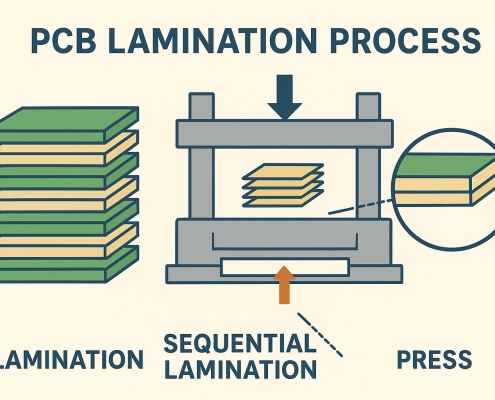 https://pcbmake.com/wp-content/uploads/2025/09/pcb-lamination.webp
1024
1536
pcbmake_admin
http://pcbmake.com/wp-content/uploads/2024/02/A去水印-1030x138.png
pcbmake_admin2025-09-04 08:10:082025-09-04 08:12:24PCB Lamination Process & Sequential Lamination
https://pcbmake.com/wp-content/uploads/2025/09/pcb-lamination.webp
1024
1536
pcbmake_admin
http://pcbmake.com/wp-content/uploads/2024/02/A去水印-1030x138.png
pcbmake_admin2025-09-04 08:10:082025-09-04 08:12:24PCB Lamination Process & Sequential Lamination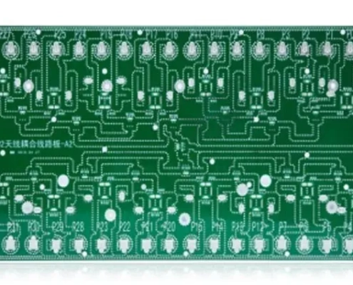 https://pcbmake.com/wp-content/uploads/2025/08/ptfe-pcb.webp
426
711
pcbmake_admin
http://pcbmake.com/wp-content/uploads/2024/02/A去水印-1030x138.png
pcbmake_admin2025-08-28 09:16:442025-08-28 09:20:46PTFE PCB: Cost, Rogers vs FR4 & Polyimide
https://pcbmake.com/wp-content/uploads/2025/08/ptfe-pcb.webp
426
711
pcbmake_admin
http://pcbmake.com/wp-content/uploads/2024/02/A去水印-1030x138.png
pcbmake_admin2025-08-28 09:16:442025-08-28 09:20:46PTFE PCB: Cost, Rogers vs FR4 & Polyimide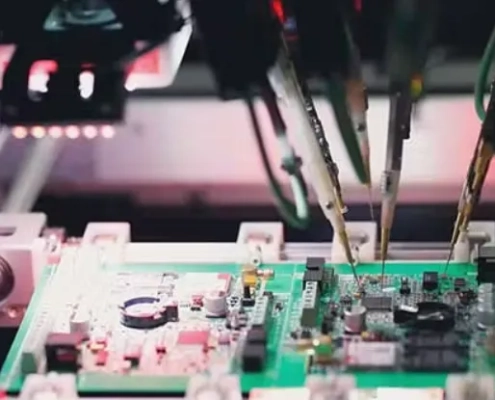 https://pcbmake.com/wp-content/uploads/2025/08/pcb-board-designer.webp
415
899
pcbmake_admin
http://pcbmake.com/wp-content/uploads/2024/02/A去水印-1030x138.png
pcbmake_admin2025-08-27 06:37:372025-08-27 06:37:37How to Test a PCB: Methods, Equipment, and Multimeter Guide
https://pcbmake.com/wp-content/uploads/2025/08/pcb-board-designer.webp
415
899
pcbmake_admin
http://pcbmake.com/wp-content/uploads/2024/02/A去水印-1030x138.png
pcbmake_admin2025-08-27 06:37:372025-08-27 06:37:37How to Test a PCB: Methods, Equipment, and Multimeter Guide https://pcbmake.com/wp-content/uploads/2025/08/pcb-manufacturing-process.webp
1536
1024
pcbmake_admin
http://pcbmake.com/wp-content/uploads/2024/02/A去水印-1030x138.png
pcbmake_admin2025-08-22 07:12:092025-08-22 07:14:17PCB Manufacturing Process: Step-by-Step Guide
https://pcbmake.com/wp-content/uploads/2025/08/pcb-manufacturing-process.webp
1536
1024
pcbmake_admin
http://pcbmake.com/wp-content/uploads/2024/02/A去水印-1030x138.png
pcbmake_admin2025-08-22 07:12:092025-08-22 07:14:17PCB Manufacturing Process: Step-by-Step Guide https://pcbmake.com/wp-content/uploads/2025/08/PTH-PCB.webp
1024
1536
pcbmake_admin
http://pcbmake.com/wp-content/uploads/2024/02/A去水印-1030x138.png
pcbmake_admin2025-08-19 07:54:002025-08-19 07:54:00PTH PCB Guide: Design, NPTH vs PTH, Vias & Components
https://pcbmake.com/wp-content/uploads/2025/08/PTH-PCB.webp
1024
1536
pcbmake_admin
http://pcbmake.com/wp-content/uploads/2024/02/A去水印-1030x138.png
pcbmake_admin2025-08-19 07:54:002025-08-19 07:54:00PTH PCB Guide: Design, NPTH vs PTH, Vias & Components https://pcbmake.com/wp-content/uploads/2025/08/pcb-xray.webp
1024
1536
pcbmake_admin
http://pcbmake.com/wp-content/uploads/2024/02/A去水印-1030x138.png
pcbmake_admin2025-08-15 08:51:132025-08-15 08:51:13PCB X-ray Inspection Machine Price, Process & AXI Guide
https://pcbmake.com/wp-content/uploads/2025/08/pcb-xray.webp
1024
1536
pcbmake_admin
http://pcbmake.com/wp-content/uploads/2024/02/A去水印-1030x138.png
pcbmake_admin2025-08-15 08:51:132025-08-15 08:51:13PCB X-ray Inspection Machine Price, Process & AXI GuideOur factory has implemented lean improvements in areas like DFM, NPI, IQC, IPQC, and OQA. These efforts have helped us achieve certifications including ISO 9001:2015, ISO 13485, IATF 16949, and SGS. Our dedication to quality and service has built long-term relationships with medium and large customers.


SHIPPING
![]()
CERTIFCATION
![]()