
Unveiling the Future: Strip Form Flip Chip Innovations
Flip chip technology represents a pivotal advancement in semiconductor packaging, revolutionizing the landscape of modern electronics. Its significance lies in its ability to enhance performance, reliability, and miniaturization of electronic devices. Flip chip ball grid array (BGA) packaging, a variant of flip chip technology, holds particular importance in semiconductor packaging. It offers increased I/O density, improved thermal performance, and enhanced electrical performance, making it ideal for high-performance applications such as CPUs, GPUs, and networking devices. Understanding the intricacies of flip chip BGA packaging is crucial for engineers and manufacturers aiming to stay at the forefront of semiconductor technology.
Understanding Flip Chip Technology: Exploring the Role of Strip Form Flip Chip BGA Substrate
Flip chip technology is a sophisticated semiconductor packaging technique that has gained immense popularity due to its numerous advantages in modern electronics. At the heart of this technology lies the intricate process flow that transforms raw wafers into fully functional integrated circuits.
The flip chip process flow begins with wafer processing, where semiconductor devices are fabricated on a silicon wafer using various lithography, etching, and deposition techniques. Once the individual chips are ready, they undergo a series of steps to prepare them for assembly onto a substrate.
Key terms in flip chip technology include:
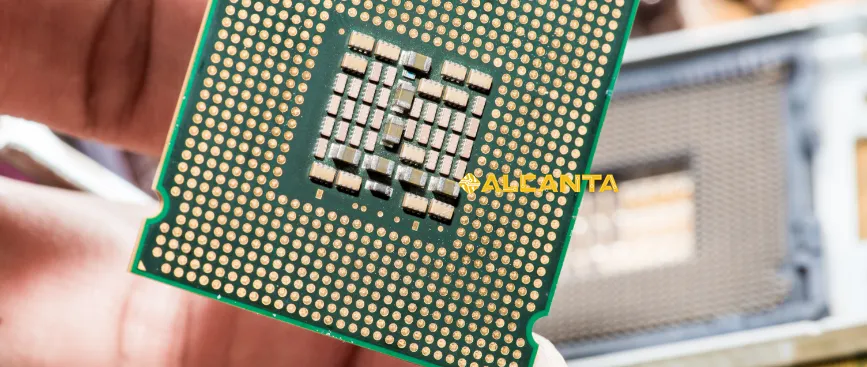
– Flip Chip: A packaging method where the active side of a semiconductor die is connected directly to the substrate or carrier using conductive bumps.
– BGA (Ball Grid Array): A type of packaging where solder balls are arranged in a grid pattern on the underside of the package, providing electrical connections to the circuit board.
– Package Substrate: The material that serves as the foundation for mounting and interconnecting semiconductor devices within a package. It provides mechanical support and electrical pathways for the integrated circuit.
– IC Substrate: A specialized substrate used in semiconductor packaging to provide a stable platform for mounting and interconnecting multiple integrated circuits.
– Staggered Pin Grid Array: A type of package where the pins are arranged in a staggered grid pattern for improved electrical performance and thermal management.
One of the most critical components in flip chip technology is the substrate material. The substrate acts as a bridge between the semiconductor die and the external environment, providing mechanical support, electrical connectivity, and thermal dissipation.
Now, let’s delve deeper into the significance of the substrate material, particularly in the context of strip form flip chip BGA substrate. This specialized substrate offers unique advantages such as improved signal integrity, enhanced thermal performance, and simplified manufacturing processes. Its design allows for efficient heat dissipation and optimized electrical pathways, making it an ideal choice for high-performance applications in various industries.
Substrate Material for Flip Chip: Exploring the Properties of Strip Form Flip Chip BGA Substrate
In flip chip technology, the substrate material plays a crucial role in ensuring the performance, reliability, and longevity of integrated circuits. Among the various substrate materials commonly used, strip form flip chip BGA substrate stands out for its unique properties and advantages.
Strip form flip chip BGA substrate typically utilizes materials such as organic substrates (e.g., FR-4), ceramics, or specialized laminates. These materials offer excellent electrical properties, mechanical strength, and thermal conductivity, making them ideal for supporting the intricate interconnections and heat dissipation requirements of flip chip packages.
The properties and characteristics of strip form flip chip BGA substrate are tailored to meet the demanding requirements of modern electronic devices. Its low electrical resistance enables efficient signal transmission, minimizing signal loss and enhancing overall performance. Additionally, the substrate’s high thermal conductivity facilitates effective heat dissipation, ensuring the reliable operation of integrated circuits under challenging conditions.
Moreover, the design flexibility of strip form flip chip BGA substrate allows for customization to meet specific application needs. Advanced manufacturing techniques enable precise patterning of electrical traces, vias, and solder mask openings, optimizing the electrical pathways and ensuring robust connectivity between the semiconductor die and external components.
Overall, strip form flip chip BGA substrate plays a pivotal role in enhancing the performance, reliability, and miniaturization of electronic devices. Its unique properties and characteristics make it a preferred choice for high-performance applications in industries such as telecommunications, automotive, and consumer electronics. By leveraging the advantages of strip form flip chip BGA substrate, manufacturers can develop innovative solutions that meet the evolving demands of the semiconductor market.
Difference Between BGA and Flip Chip: Navigating Packaging Technologies
Understanding the distinctions between BGA (Ball Grid Array) and flip chip packaging technologies is essential for engineers and manufacturers seeking optimal solutions for semiconductor packaging. While both methods serve to connect integrated circuits to substrates, they differ significantly in structure, assembly process, and application scenarios.
Structure:
– BGA: In BGA packaging, solder balls are arranged in a grid pattern on the underside of the package. The integrated circuit is typically mounted on top of the substrate, and electrical connections are made through the solder balls.
– Flip Chip: In flip chip packaging, the active side of the semiconductor die is flipped and directly bonded to the substrate or carrier using conductive bumps, such as solder bumps or copper pillars.
Assembly Process:
– BGA: The assembly process for BGA packages involves soldering the package onto the substrate using reflow soldering techniques. The solder balls melt and form connections between the package and the substrate.
– Flip Chip: The flip chip assembly process entails precisely aligning the semiconductor die with the substrate and bonding them together using conductive bumps. This process may involve flip chip bonder equipment and underfill material to enhance mechanical stability.
Application Scenarios:
– BGA: BGA packaging is commonly used in applications where moderate to high I/O (Input/Output) density is required, such as consumer electronics, networking devices, and automotive electronics. It offers relatively simple assembly and robust mechanical connections.
– Flip Chip: Flip chip packaging is preferred for high-performance applications that demand superior electrical and thermal performance, such as CPUs, GPUs, and high-speed communication devices. It enables shorter electrical paths, reduced parasitic capacitance, and improved thermal dissipation compared to BGA.
Advantages and Disadvantages:
– BGA:
– Advantages: Moderate to high I/O density, simpler assembly process, robust mechanical connections.
– Disadvantages: Limited electrical and thermal performance compared to flip chip, susceptibility to solder joint fatigue under thermal cycling.
– Flip Chip:
– Advantages: Superior electrical and thermal performance, shorter electrical paths, reduced parasitic capacitance, enhanced thermal dissipation.
– Disadvantages: Complex assembly process, higher manufacturing costs, potential for solder joint reliability issues under mechanical stress.
In summary, while BGA and flip chip packaging technologies share the common goal of connecting integrated circuits to substrates, they offer distinct advantages and are suited for different application scenarios. By carefully considering the requirements of a particular application, engineers can choose the most appropriate packaging technology to optimize performance, reliability, and cost-effectiveness.
The Substrate of BGA: Unveiling its Crucial Role
In BGA (Ball Grid Array) packaging, the substrate material serves as the foundation upon which the integrated circuit (IC) is mounted, providing essential support and connectivity for the device. Understanding the substrate material used in BGA packages and its impact on overall package performance is fundamental to optimizing the design and reliability of electronic systems.
Explanation of the Substrate Material:
The substrate material commonly used in BGA packages varies depending on the specific application requirements and performance objectives. Typically, organic substrates such as fiberglass-reinforced epoxy (FR-4) or specialized laminates are utilized due to their favorable electrical, mechanical, and thermal properties. These materials offer excellent dielectric properties, allowing efficient signal transmission while providing mechanical stability to the package. Additionally, the substrate material must exhibit good thermal conductivity to dissipate heat generated by the IC, ensuring reliable operation under varying environmental conditions.
Role of the Substrate in BGA Packaging:
The substrate in BGA packaging plays several critical roles that contribute to the overall performance and reliability of the integrated circuit:
1. Mechanical Support: The substrate serves as a sturdy platform for mounting the IC and other components, ensuring proper alignment and structural integrity of the package.
2. Electrical Connectivity: The substrate facilitates electrical connections between the IC and the external circuitry, allowing signals to be transmitted and received effectively. It consists of a network of conductive traces and vias that route signals between the IC and the solder balls.
3. Heat Dissipation: The substrate material’s thermal conductivity enables efficient heat dissipation from the IC to the surrounding environment, preventing overheating and maintaining optimal operating temperatures. This is particularly crucial for high-power applications where thermal management is essential to prevent performance degradation and reliability issues.
Impact on Overall Package Performance:
The choice of substrate material significantly influences the electrical, mechanical, and thermal performance of the BGA package:
– Electrical Performance: The substrate’s dielectric properties and interconnect design affect signal integrity, propagation delay, and crosstalk, ultimately impacting the circuit’s speed and reliability.
– Mechanical Reliability: The substrate’s mechanical strength and dimensional stability ensure the package withstands mechanical stresses, such as thermal cycling and mechanical shock, without compromising its structural integrity.
– Thermal Management: The substrate’s thermal conductivity and heat dissipation capabilities determine the package’s ability to dissipate heat generated by the IC, preventing thermal-induced failures and ensuring long-term reliability.
In conclusion, the substrate material used in BGA packages plays a pivotal role in ensuring the overall performance, reliability, and longevity of integrated circuits. By carefully selecting and optimizing the substrate material, engineers can design BGA packages that meet the stringent requirements of various applications while maintaining high levels of performance and reliability.
Difference Between CSP and Flip Chip: Navigating Packaging Technologies
Chip scale packaging (CSP) and flip chip technology are both advanced semiconductor packaging techniques, but they have distinct characteristics and serve different purposes in electronic systems. Understanding the differences between them is crucial for engineers and manufacturers seeking optimal solutions for various applications.
Differentiating between CSP and Flip Chip Technology:
– CSP: Chip scale packaging is a packaging method where the size of the package is comparable to that of the integrated circuit (IC) chip itself. CSP eliminates the need for additional packaging material, resulting in a compact form factor that minimizes the footprint of the device.
– Flip Chip: Flip chip technology, on the other hand, involves directly bonding the active side of the IC chip to the substrate or carrier using conductive bumps. This method offers superior electrical and thermal performance compared to traditional wire bonding techniques.
Comparison of Form Factors, Assembly Methods, and Applications:
– Form Factors: CSP packages are typically smaller and have a lower profile compared to flip chip packages. They are designed to be as close to the size of the IC chip as possible, maximizing space utilization on the printed circuit board (PCB). Flip chip packages, while also compact, may include additional substrate material and solder balls, resulting in slightly larger dimensions.
– Assembly Methods: CSP packages are often assembled using surface mount technology (SMT) processes, where the package is soldered directly onto the PCB using reflow soldering techniques. Flip chip packages require more precise alignment and bonding processes, often involving specialized flip chip bonder equipment and underfill materials to enhance mechanical stability.
– Applications: CSP is commonly used in portable electronic devices, such as smartphones, tablets, and wearables, where space constraints are critical. Flip chip technology is preferred for high-performance applications that demand superior electrical and thermal performance, such as microprocessors, graphics processing units (GPUs), and high-speed communication devices.
Discussing Substrate Material Differences:
– The substrate material used in CSP packages is typically a thin laminate or organic substrate, chosen for its compactness and low profile. These substrates may offer limited thermal conductivity and mechanical strength compared to those used in flip chip packages.
– Flip chip packages often utilize more robust substrate materials, such as ceramics or specialized laminates, to accommodate the higher heat dissipation requirements and mechanical stresses associated with flip chip bonding. These substrates offer enhanced thermal conductivity and mechanical stability, ensuring reliable performance under demanding conditions.
In summary, while both CSP and flip chip technologies offer compact packaging solutions for semiconductor devices, they differ in form factors, assembly methods, and applications. By understanding these differences and selecting the appropriate packaging technology and substrate material, engineers can optimize the performance, reliability, and manufacturability of electronic systems for diverse applications.
Introducing Strip Form Flip Chip BGA Substrate: Revolutionizing Semiconductor Packaging
In the realm of semiconductor packaging, strip form flip chip BGA substrate represents a cutting-edge innovation that offers significant advancements in performance, reliability, and miniaturization. Let’s delve into the definition, significance, unique features, and potential impact of this transformative technology.
Definition and Significance:
Strip form flip chip BGA substrate refers to a specialized substrate design tailored for flip chip BGA packages, where the substrate material is configured in a strip or linear form factor. This innovative approach optimizes the arrangement of conductive traces, vias, and solder mask openings, enhancing electrical performance, signal integrity, and thermal management in flip chip packages. Its significance lies in its ability to address the evolving demands of high-performance applications while offering simplified manufacturing processes and cost efficiencies.
Unique Features and Benefits:
– Enhanced Electrical Performance: The strip form substrate minimizes signal propagation distances, reducing parasitic capacitance and signal loss, thereby improving electrical performance and transmission speed.
– Optimized Thermal Management: By optimizing the layout and design of the substrate, strip form flip chip BGA packages achieve superior thermal dissipation, effectively managing heat generated by the integrated circuit and ensuring reliable operation under challenging thermal conditions.
– Simplified Manufacturing Processes: The linear arrangement of components on the strip form substrate streamlines assembly processes, reducing manufacturing complexities and enhancing production efficiency. This results in cost savings and faster time-to-market for semiconductor devices.
Applications and Potential Impact:
– High-Performance Computing: Strip form flip chip BGA substrate is well-suited for high-performance computing applications, including CPUs, GPUs, and server processors, where superior electrical performance and thermal management are critical for achieving optimal performance.
– Networking and Telecommunications: In networking and telecommunications equipment, strip form flip chip BGA packages enable high-speed data transmission and reliable connectivity, enhancing the efficiency and reliability of communication systems.
– Automotive Electronics: The robust design and thermal stability of strip form flip chip BGA substrate make it an ideal choice for automotive electronics, where reliability and durability are paramount in harsh operating environments.
The introduction of strip form flip chip BGA substrate is poised to revolutionize the semiconductor packaging industry by offering unparalleled performance, reliability, and versatility. As demand for high-performance electronic devices continues to grow across various industries, this innovative technology is expected to play a pivotal role in driving advancements in semiconductor packaging and enabling the development of next-generation electronic systems.
FAQs about strip form flip chip bga substrate
The substrate material for flip chip can vary but commonly includes organic substrates like FR-4, ceramics, or specialized laminates. These materials provide mechanical support, electrical connectivity, and thermal dissipation for the integrated circuit.
The main difference between BGA and flip chip lies in their structure and assembly method. In BGA packaging, solder balls are arranged in a grid pattern on the underside of the package, while in flip chip packaging, the active side of the semiconductor die is directly bonded to the substrate using conductive bumps. BGA typically involves soldering the package onto the substrate, while flip chip bonding requires precise alignment and bonding of the semiconductor die to the substrate.
The substrate of BGA typically consists of materials such as organic substrates (e.g., FR-4), ceramics, or specialized laminates. This substrate provides mechanical support and electrical pathways for mounting and interconnecting semiconductor devices within the package.
The difference between CSP (Chip Scale Packaging) and flip chip lies in their form factor, assembly methods, and applications. CSP packages are designed to be as close to the size of the IC chip as possible, eliminating the need for additional packaging material. They are typically assembled using surface mount technology (SMT) processes. In contrast, flip chip technology involves directly bonding the active side of the IC chip to the substrate using conductive bumps and may require specialized flip chip bonder equipment. Flip chip technology is preferred for high-performance applications that demand superior electrical and thermal performance, while CSP is commonly used in portable electronic devices where space constraints are critical.

