
Essential Insights: Flip Chip Packaging Substrate Manufacturer
In the dynamic landscape of semiconductor packaging, flip chip technology stands as a pivotal innovation. This advanced packaging method offers superior performance, increased reliability, and enhanced miniaturization compared to conventional methods. Central to the success of flip chip packaging is the substrate, serving as the foundation for interconnection and structural support. As such, the substrate plays a critical role in ensuring the functionality and longevity of integrated circuits. In this article, we delve into the intricate world of flip chip packaging substrates, emphasizing the indispensable role played by flip chip packaging substrate manufacturers. These manufacturers are instrumental in providing cutting-edge materials and technologies tailored to meet the stringent demands of modern semiconductor packaging processes.
Understanding the Role of Flip Chip Packaging Substrate Manufacturers
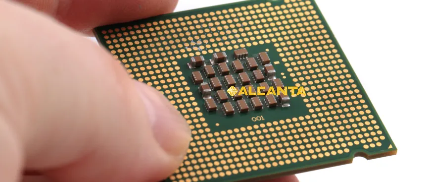
Defining Flip Chip Packaging Substrate A flip chip packaging substrate refers to the foundational material on which the integrated circuit (IC) is mounted and interconnected in a flip chip packaging process. Unlike traditional wire bonding methods, flip chip technology involves directly attaching the IC to the substrate, allowing for a more compact and efficient design.
Properties and Characteristics Required in Flip Chip Substrates
- Thermal Management: Flip chip substrates must possess excellent thermal conductivity to dissipate heat generated by the IC effectively. This ensures optimal performance and reliability of the packaged device.
- Electrical Properties: Low dielectric constant (Dk) and low signal loss characteristics are essential for maintaining signal integrity and minimizing electrical noise in high-speed applications.
- Mechanical Strength: The substrate material should exhibit high mechanical strength to withstand stresses during manufacturing processes and operation.
- Dimensional Stability: Flip chip substrates must maintain dimensional stability under varying temperature and humidity conditions to prevent warpage and ensure proper alignment of the IC.
- Compatibility with Assembly Processes: Substrates should be compatible with flip chip assembly processes, including solder reflow, underfill encapsulation, and testing procedures.
Importance of Substrate Material Selection The selection of substrate material is critical in determining the performance, reliability, and manufacturability of flip chip packages. Flip chip packaging substrate manufacturers play a pivotal role in offering a diverse range of materials tailored to meet specific application requirements. Factors influencing material selection include:
- Thermal conductivity
- Electrical properties
- Cost-effectiveness
- Availability of advanced packaging technologies
- Compatibility with assembly processes
- Environmental considerations
The expertise of flip chip packaging substrate manufacturers in material science and engineering enables them to develop innovative solutions that address the evolving needs of the semiconductor industry. Collaborative partnerships between manufacturers and semiconductor companies facilitate the customization and optimization of substrate materials for enhanced performance and reliability in flip chip packaging applications.
Understanding the Role of Flip Chip Packaging Substrate Manufacturers
Overview of Leading Semiconductor Substrate Manufacturers
Several prominent companies specialize in the production of substrates tailored for flip chip packaging applications. These include established players with extensive experience in semiconductor materials and advanced packaging technologies. Some notable semiconductor substrate manufacturers include:
- Amkor Technology: Amkor is a global leader in semiconductor packaging and test services, offering a comprehensive portfolio of substrate solutions optimized for flip chip packaging. Their expertise spans various substrate materials, including organic substrates, laminate substrates, and advanced interconnect technologies.
- Taiwan Semiconductor Manufacturing Company (TSMC): TSMC is renowned for its semiconductor manufacturing capabilities, but it also plays a significant role in providing advanced substrate solutions for flip chip packaging. Leveraging its cutting-edge fabrication facilities and research expertise, TSMC develops high-performance substrates tailored to meet the demanding requirements of next-generation integrated circuits.
- ASE Technology Holding Co., Ltd.: ASE is a leading provider of semiconductor packaging and test services, offering a diverse range of substrate solutions for flip chip packaging applications. With a strong focus on innovation and collaboration, ASE delivers advanced substrate technologies that enable enhanced performance, reliability, and miniaturization in electronic devices.
- Kyocera Corporation: Kyocera specializes in the development and manufacturing of ceramic substrates for various electronic applications, including flip chip packaging. Their expertise in ceramic materials and precision manufacturing processes enables the production of high-quality substrates with exceptional thermal and electrical properties.
Their Role in the Supply Chain of Flip Chip Packaging
Flip chip packaging substrate manufacturers play a crucial role in the supply chain of semiconductor packaging. They collaborate closely with semiconductor companies, packaging subcontractors, and end customers to deliver customized substrate solutions that meet specific application requirements. Key aspects of their role include:
- Research and Development: Semiconductor substrate manufacturers invest in research and development to continuously improve substrate materials, design, and manufacturing processes. This involves exploring new materials, optimizing fabrication techniques, and enhancing substrate performance to address emerging trends and challenges in flip chip packaging.
- Customization and Optimization: Substrate manufacturers work closely with semiconductor companies to understand their unique packaging requirements and tailor substrate solutions accordingly. This may involve customizing substrate materials, dimensions, and electrical properties to ensure compatibility with specific IC designs and performance targets.
- Quality Assurance and Reliability: Ensuring the quality and reliability of flip chip substrates is paramount in semiconductor packaging. Substrate manufacturers implement stringent quality control measures and reliability testing protocols to verify the performance and durability of their products. This includes evaluating substrate materials for thermal stability, mechanical strength, electrical conductivity, and long-term reliability under operating conditions.
- Supply Chain Management: Semiconductor substrate manufacturers manage complex supply chains to procure raw materials, fabricate substrates, and deliver finished products to customers on time. This involves collaborating with material suppliers, manufacturing partners, and logistics providers to optimize supply chain efficiency, minimize lead times, and ensure product availability.
Flip chip packaging substrate manufacturers play a critical role in the semiconductor supply chain, providing essential substrate solutions that enable the development of advanced integrated circuits with enhanced performance, reliability, and miniaturization. Their expertise in substrate materials, design, and manufacturing processes drives innovation and facilitates the adoption of flip chip packaging technologies across various electronic applications.
Flip Chip Packaging Process
Step-by-step Explanation of the Flip Chip Packaging Process
- Wafer Preparation: The process begins with the fabrication of semiconductor wafers containing numerous individual integrated circuits (ICs). These wafers undergo various processing steps, including lithography, etching, and deposition, to create the desired circuitry.
- Wafer Testing: Once the circuits are fabricated, the wafer undergoes testing to identify and eliminate defective ICs. This ensures that only functional ICs are used in the packaging process, improving overall yield and reliability.
- Die Attach: In this step, the individual ICs (also known as dies) are picked from the wafer and attached to the substrate or carrier using die attach adhesive. The substrate provides mechanical support and electrical interconnection for the die.
- Flip Chip Bonding: The die is flipped over and aligned with the corresponding bonding pads on the substrate. A solder bump or conductive adhesive is used to create electrical connections between the die and substrate. This process is typically performed using automated equipment with high precision to ensure accurate alignment and reliable bonding.
- Underfill Encapsulation: After flip chip bonding, an underfill material is dispensed around the perimeter of the die to provide mechanical reinforcement and protect the solder joints from mechanical stress and moisture ingress. The underfill material is then cured to form a solid encapsulant.
- Curing and Testing: The assembly undergoes curing to ensure the proper adhesion and curing of the underfill material. Subsequent testing is conducted to verify the electrical functionality and reliability of the packaged device. This may include electrical testing, thermal cycling, and mechanical stress testing.
- Final Packaging: Once testing is complete, the packaged devices are singulated into individual units and packaged into final packages, such as plastic or ceramic packages. These packages provide additional protection and facilitate integration into electronic systems.
Role of the Substrate in Each Step of the Process
- Wafer Preparation: Although the substrate is not directly involved in this step, its properties and characteristics influence the design and fabrication of the ICs on the wafer.
- Die Attach: The substrate serves as the mounting platform for the die during the die attach process. It provides mechanical support and stability to ensure proper alignment and bonding of the die.
- Flip Chip Bonding: The substrate plays a crucial role in flip chip bonding by providing the electrical interconnection between the die and the external circuitry. It also influences the thermal and electrical performance of the packaged device.
- Underfill Encapsulation: The substrate serves as the foundation for dispensing and curing the underfill material. It helps to encapsulate the solder joints and protect them from mechanical stress and environmental factors.
- Curing and Testing: The substrate provides structural support during the curing process and facilitates the electrical testing of the packaged device. It ensures that the device remains stable and intact during testing procedures.
- Final Packaging: The substrate may also influence the selection and design of the final package used to encapsulate the packaged device. It plays a role in determining the overall size, shape, and performance of the final packaged device.
Leadframe vs Substrate: A Comparative Analysis
Understanding the Differences between Leadframe and Substrate in Packaging
- Leadframe:
- Definition: A leadframe is a thin metal frame that provides electrical connections for semiconductor devices. It typically consists of a grid of metal leads connected to a die pad, which serves as the mounting platform for the semiconductor die.
- Construction: Leadframes are usually made of metals such as copper, copper alloys, or iron-nickel alloys. They are manufactured using stamping or etching processes to create the desired lead pattern.
- Assembly Process: In leadframe-based packaging, the semiconductor die is mounted onto the die pad of the leadframe. Wire bonding is then used to connect the bond pads on the die to the leads of the leadframe.
- Applications: Leadframe packaging is commonly used in traditional semiconductor packaging applications, such as dual in-line packages (DIPs), quad flat packages (QFPs), and small outline integrated circuits (SOICs).
- Substrate:
- Definition: A substrate is a material (typically organic or ceramic) used as the foundation for mounting and interconnecting semiconductor devices in advanced packaging technologies such as flip chip and ball grid array (BGA) packaging.
- Construction: Substrates can be made of various materials, including organic laminates, ceramics, and metal-core laminates. They are manufactured using processes such as lamination, drilling, and etching to create the necessary circuitry and interconnects.
- Assembly Process: In substrate-based packaging, the semiconductor die is typically flip-chip bonded or wire bonded directly onto the substrate. Interconnects are then formed between the die and the substrate using solder bumps or conductive traces.
- Applications: Substrate-based packaging is widely used in modern semiconductor packaging technologies, including flip chip packages, chip-scale packages (CSPs), and system-in-package (SiP) modules.
Advantages and Disadvantages of Each Approach
- Leadframe:
- Advantages:
- Cost-effective for high-volume production.
- Established manufacturing processes and supply chain.
- Good thermal and electrical conductivity.
- Disadvantages:
- Limited I/O density and package size.
- Less suitable for high-speed and high-density applications.
- Susceptible to wire bond reliability issues such as bond lifting and wire sweep.
- Advantages:
- Substrate:
- Advantages:
- High I/O density and package size scalability.
- Superior thermal and electrical performance.
- Compatibility with advanced packaging technologies such as flip chip.
- Disadvantages:
- Higher initial cost compared to leadframes.
- Complex manufacturing processes requiring advanced equipment and expertise.
- Limited availability of substrate materials for certain applications.
- Advantages:
The choice between leadframe and substrate-based packaging depends on factors such as package size, I/O density, performance requirements, and cost considerations. While leadframes offer cost-effective solutions for standard packaging applications, substrates provide greater flexibility and performance advantages for advanced packaging technologies requiring higher density and enhanced thermal and electrical performance.
Embedded Trace Substrate: Innovations in Flip Chip Packaging
Overview of Embedded Trace Substrates and Their Significance
Embedded trace substrates represent a cutting-edge advancement in flip chip packaging technology. Unlike traditional substrates, embedded trace substrates integrate signal traces directly within the substrate material itself, eliminating the need for additional wiring layers. This innovative approach enables higher routing densities, reduced signal path lengths, and enhanced signal integrity in flip chip packages.
How Embedded Trace Substrates Enhance Performance and Reliability
- Improved Signal Integrity: By embedding signal traces within the substrate, embedded trace substrates minimize signal propagation delays, impedance mismatches, and signal crosstalk. This results in improved signal integrity and reduced susceptibility to noise, allowing for higher-speed operation and more reliable data transmission.
- Enhanced Thermal Management: Embedded trace substrates offer superior thermal conductivity compared to traditional substrates, thanks to the absence of additional wiring layers. This enables more efficient heat dissipation from the integrated circuit (IC), reducing the risk of thermal issues such as hot spots and ensuring optimal performance under various operating conditions.
- Miniaturization and Space Savings: The elimination of external wiring layers in embedded trace substrates allows for more compact and space-efficient flip chip packages. This is particularly beneficial for applications where size and weight constraints are critical, such as mobile devices, wearables, and automotive electronics.
- Increased Design Flexibility: Embedded trace substrates offer greater design flexibility compared to traditional substrates, as signal traces can be routed directly within the substrate material. This enables more intricate and optimized layouts, accommodating complex IC designs and high-density interconnect requirements without compromising performance or reliability.
- Enhanced Reliability: By reducing the number of external wiring layers and interconnects, embedded trace substrates minimize the risk of electrical shorts, opens, and other reliability issues commonly associated with traditional flip chip packaging methods. This results in improved long-term reliability and durability of the packaged devices, reducing the likelihood of premature failures and enhancing product lifespan.
In summary, embedded trace substrates represent a significant advancement in flip chip packaging technology, offering numerous benefits in terms of performance, reliability, miniaturization, and design flexibility. As the demand for high-performance and compact electronic devices continues to grow, embedded trace substrates are poised to play a pivotal role in meeting the evolving needs of the semiconductor industry.
FAQs About Flip chip packaging substrate manufacturer
The substrate of flip chip packaging is a material, often organic or ceramic, that serves as the foundation for mounting and interconnecting semiconductor devices in flip chip packaging technology. It provides mechanical support and electrical interconnection for the integrated circuit (IC) during the packaging process.
In chip manufacturing, a substrate refers to the material on which semiconductor devices are fabricated or mounted. It acts as a base for building the various layers and components of the chip. The substrate provides structural support and electrical connections for the semiconductor devices, facilitating their integration into electronic systems.
The flip chip packaging process involves directly attaching the active surface of a semiconductor die (integrated circuit) to a substrate or carrier using conductive bumps, typically made of solder or conductive adhesive. This process allows for a more compact and efficient packaging design compared to traditional wire bonding methods.
The process of flip chip manufacturing encompasses several steps:
a. Wafer preparation: Fabrication of semiconductor wafers containing multiple individual ICs.
b. Die attach: Mounting the ICs onto the substrate or carrier.
c. Flip chip bonding: Flipping the ICs over and aligning them with bonding pads on the substrate, followed by creating electrical connections using solder bumps or conductive adhesive.
d. Underfill encapsulation: Dispensing and curing an underfill material around the die to provide mechanical reinforcement and protect the solder joints.
e. Curing and testing: Curing the underfill material and conducting electrical testing to verify the functionality and reliability of the packaged device.
f. Final packaging: Singulating the packaged devices into individual units and encapsulating them into final packages, such as plastic or ceramic packages, for further integration into electronic systems.

