
Mastering the Art of BGA Substrate Design
In the ever-evolving landscape of electronics, Ball Grid Array (BGA) technology stands as a cornerstone of innovation. This compact and efficient packaging solution has revolutionized the way electronic components are interconnected, offering higher density and improved thermal performance. However, beneath the surface of BGA lies a crucial element often overlooked: substrate design. The substrate serves as the foundation for BGA, facilitating electrical connections while managing heat dissipation and ensuring signal integrity. Recognizing the pivotal role of substrate design is paramount, as it directly impacts the performance, reliability, and manufacturability of BGA-based systems. Thus, delving into the intricacies of BGA substrate design becomes imperative for engineers and designers striving to unleash the full potential of modern electronics.
Understanding BGA Substrate Design
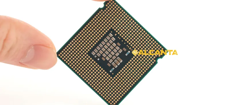
Ball Grid Array (BGA) substrate serves as the platform upon which the intricate network of connections within electronic devices is built. It acts as the intermediary between the silicon die and the printed circuit board (PCB), providing electrical pathways for signals to travel and facilitating the dissipation of heat generated by the integrated circuits.
Definition of BGA Substrate:
A BGA substrate is a specialized substrate material typically made of a laminate or ceramic material, with a grid of conductive pads arranged in a regular array on one side. These pads serve as the connection points for solder balls that attach the BGA package to the PCB.
Role in Electronic Packaging:
The BGA substrate plays a crucial role in electronic packaging by providing a stable platform for mounting integrated circuits (ICs) and ensuring reliable electrical connections between the ICs and the PCB. It also aids in dissipating heat generated by the ICs to prevent overheating and maintain optimal operating conditions.
Key Components and Layout Considerations:
Several components contribute to the design of a BGA substrate, including the substrate material, routing layers, vias, and solder mask. Layout considerations include pad pitch, via placement, signal routing, and power distribution. These elements must be carefully optimized to achieve optimal electrical performance, thermal management, and manufacturability.
Importance of Thermal Management:
Effective thermal management is critical in BGA substrate design to prevent ICs from overheating, which can lead to performance degradation or even failure. Thermal vias, heat sinks, and thermal pads are commonly employed to efficiently dissipate heat away from the ICs and distribute it across the substrate.
Importance of Signal Integrity:
Signal integrity refers to the ability of signals to retain their quality and integrity as they propagate through the BGA substrate and PCB. Proper substrate design, including controlled impedance routing, signal isolation, and minimizing crosstalk, is essential to maintain signal integrity and ensure reliable communication between ICs.
Importance of Manufacturability:
Manufacturability considerations encompass the ease and efficiency of producing BGA substrates in large quantities while maintaining consistent quality. Factors such as substrate material selection, fabrication processes, and assembly techniques impact the manufacturability of BGA substrates and ultimately influence the overall cost and reliability of electronic devices.
Rules for BGA Substrate Design
Designing a BGA substrate requires adherence to a set of rigorous rules and guidelines to ensure optimal performance, reliability, and manufacturability. Here’s a detailed examination of the key aspects:
1. Design Rules and Guidelines:
– Pad Layout: The arrangement and size of pads must adhere to specified pitch and diameter requirements. Pad pitch determines the spacing between pads, while pad diameter affects solder joint reliability.
– Via Design: Vias are crucial for connecting different layers of the substrate. Proper via size, placement, and aspect ratio are essential to maintain signal integrity and thermal performance.
– Routing: Trace routing must consider signal integrity, impedance matching, and noise immunity. Differential pairs should be routed close together with consistent spacing to minimize signal skew.
– Spacing Requirements: Adequate spacing between pads and traces is necessary to prevent electrical shorting and ensure manufacturability. Spacing requirements vary based on package size, pitch, and electrical characteristics.
2. Pad Layout:
– Pad Pitch: The distance between the centers of adjacent pads determines the pitch. Smaller pitches allow for higher pin density but may require more precise manufacturing processes.
– Pad Diameter: The diameter of the pad impacts solder joint reliability and electrical performance. Proper pad diameter selection ensures adequate solder wetting and mechanical strength.
3. Via Design:
– Via Size: Vias should be sized appropriately to accommodate the required signal and power connections. Smaller vias may be used for signal routing, while larger vias are necessary for power and thermal vias.
– Via Placement: Strategic placement of vias is crucial to minimize signal distortion and maintain signal integrity. Vias should be placed to minimize impedance mismatches and signal reflections.
4. Routing:
– Signal Integrity: Signal traces should be routed to minimize impedance variations, crosstalk, and signal skew. Differential pairs should be routed symmetrically to maintain signal integrity and minimize electromagnetic interference (EMI).
– Power Distribution: Proper power distribution is essential to ensure stable operation of the ICs. Power traces should be routed to minimize voltage drops and noise.
5. Adherence to Industry Standards:
– Compliance with industry standards, such as IPC-7095 for BGA design and IPC-2221 for PCB design, is essential to ensure reliability and interoperability.
– Following established guidelines and best practices helps mitigate risks associated with manufacturing defects, reliability issues, and performance degradation.
Adhering to these rules and guidelines is critical for achieving high-quality BGA substrates that meet stringent reliability and performance requirements in modern electronic applications.
The Substrate of BGA
The substrate of a BGA (Ball Grid Array) plays a pivotal role in determining the overall performance and reliability of electronic devices. Let’s delve deeper into the intricacies of BGA substrate materials, their properties, and their impact on electrical performance and thermal dissipation:
1. Materials Used in BGA Substrates:
– FR-4 Laminate: FR-4 is a common substrate material known for its affordability and availability. It is composed of a woven glass fabric impregnated with epoxy resin. FR-4 offers good electrical insulation and mechanical strength, making it suitable for many applications.
– High-Speed Laminate: High-speed laminates, such as polyimide or PTFE (Teflon), are preferred for applications requiring high-frequency operation. These materials exhibit low dielectric loss and excellent signal integrity, making them ideal for high-speed data transmission.
– Ceramic Substrates: Ceramic substrates, typically composed of alumina (Al2O3) or aluminum nitride (AlN), offer superior thermal conductivity compared to organic materials. Ceramic substrates excel in thermal management, making them suitable for high-power applications or devices operating in harsh environments.
2. Comparison Between Substrate Materials:
– Electrical Properties: High-speed laminates offer superior electrical performance, with lower dielectric constants and lower signal loss compared to FR-4. Ceramic substrates also exhibit excellent electrical properties, especially at high frequencies.
– Thermal Properties: Ceramic substrates have significantly higher thermal conductivity than organic materials like FR-4, enabling efficient heat dissipation. High-speed laminates may have moderate thermal conductivity, depending on their composition.
– Cost and Availability: FR-4 is cost-effective and widely available, making it suitable for most consumer electronics. High-speed laminates and ceramic substrates are more expensive and may have limited availability, particularly for specialized applications.
3. Impact on Electrical Performance and Thermal Dissipation:
– Electrical Performance: The choice of substrate material directly affects signal integrity, impedance control, and noise immunity. High-speed laminates and ceramic substrates offer superior electrical performance, minimizing signal distortion and transmission losses.
– Thermal Dissipation: Ceramic substrates excel in thermal management, efficiently dissipating heat away from the ICs and reducing the risk of overheating. High-speed laminates may require additional thermal management techniques, such as thermal vias or heat sinks, to mitigate heat buildup.
In conclusion, the selection of BGA substrate material is a critical decision that influences the electrical performance, thermal management, and overall reliability of electronic devices. Engineers must carefully evaluate the requirements of their specific application to choose the most suitable substrate material for optimal performance.
Disadvantages of BGA
While Ball Grid Array (BGA) technology offers numerous advantages, it is not without its drawbacks. Let’s explore these disadvantages in detail, along with strategies to mitigate them:
1. Reworkability:
– BGA packages pose challenges for rework and repair due to their compact size and hidden solder joints. Removing and replacing a defective BGA component without damaging adjacent components can be complex and time-consuming.
– Strategies to mitigate reworkability issues include implementing advanced rework techniques such as hot air rework stations, X-ray inspection for accurate solder joint analysis, and the use of rework stencils for precise solder paste application during rework processes.
2. Inspection Difficulty:
– Traditional visual inspection methods are inadequate for detecting defects in BGA solder joints, as the joints are often hidden beneath the package. This makes it challenging to identify issues such as insufficient solder, voids, or cracks.
– Advanced inspection techniques such as X-ray inspection, acoustic microscopy, and automated optical inspection (AOI) systems are employed to inspect BGA solder joints with higher accuracy and reliability. These techniques provide detailed insights into the quality of solder joints and help detect defects early in the manufacturing process.
3. Cost:
– BGA packages typically cost more than traditional surface-mount devices (SMDs) due to their complex design, higher material costs, and specialized manufacturing processes. Additionally, the equipment and expertise required for BGA assembly and inspection add to the overall cost.
– Cost-saving strategies include optimizing BGA substrate design to minimize material usage, streamlining manufacturing processes for efficiency, and leveraging economies of scale through bulk purchasing and strategic supplier partnerships.
4. Strategies to Mitigate Disadvantages:
– Optimized Substrate Design: Designing BGA substrates with robust thermal management features, well-defined routing paths, and optimized pad layouts can enhance reliability and ease of manufacturing.
– Advanced Manufacturing Processes: Employing advanced manufacturing techniques such as laser drilling for precise via formation, automated solder paste deposition for consistent soldering, and automated optical inspection for quality control can improve process efficiency and yield.
– Supplier Collaboration: Collaborating closely with substrate and component suppliers to ensure quality materials, streamlined logistics, and continuous improvement initiatives can help mitigate risks and reduce costs.
– Continuous Improvement: Regularly evaluating and optimizing manufacturing processes, inspection methodologies, and design practices through continuous improvement initiatives can lead to enhanced product quality, cost savings, and customer satisfaction.
In conclusion, while BGA technology presents challenges such as reworkability, inspection difficulty, and cost, these drawbacks can be effectively mitigated through strategic approaches focusing on optimized substrate design, advanced manufacturing processes, supplier collaboration, and continuous improvement efforts. By addressing these challenges proactively, manufacturers can maximize the benefits of BGA technology while minimizing associated risks.
Spacing for BGA Pads
The spacing between pads in a Ball Grid Array (BGA) design is a critical aspect that directly impacts electrical performance, manufacturability, and reliability. Let’s delve into the importance of pad spacing, factors influencing spacing requirements, and optimal strategies for different BGA applications and package sizes:
1. Importance of Pad Spacing in BGA Design:
– Pad spacing determines the distance between adjacent solder balls, affecting the overall pitch and density of the BGA package.
– Adequate pad spacing is essential to prevent electrical shorting between adjacent pads during soldering and operation, ensuring signal integrity and reliability.
– Optimal pad spacing facilitates efficient soldering processes, inspection, and reworkability, contributing to overall manufacturing yield and cost-effectiveness.
2. Factors Influencing Pad Spacing Requirements:
– Pitch Size: The pitch size, or the distance between the centers of adjacent solder balls, is a primary determinant of pad spacing. Smaller pitch sizes typically require tighter pad spacing to accommodate the increased number of pads within a limited area.
– Electrical Considerations: Pad spacing must consider electrical characteristics such as signal routing, impedance control, and power distribution. Maintaining adequate spacing between signal pads minimizes crosstalk and signal interference, while spacing between power and ground pads influences power integrity and thermal management.
– Manufacturability: Pad spacing affects the manufacturability of BGA packages, including solder paste deposition, solder ball attachment, and inspection processes. Balancing pad spacing with manufacturability considerations is crucial to achieve high yields and consistent quality.
3. Optimal Spacing Strategies for Different BGA Applications and Package Sizes:
– Fine-Pitch BGAs: For fine-pitch BGAs with small pitch sizes (e.g., less than 0.8 mm), tight pad spacing is necessary to accommodate the high density of solder balls. However, care must be taken to ensure sufficient clearance between pads to prevent solder bridging and ensure manufacturability.
– Standard-Pitch BGAs: Standard-pitch BGAs with larger pitch sizes (e.g., 0.8 mm or greater) allow for more relaxed pad spacing while maintaining electrical and thermal performance. This provides greater flexibility in layout and reduces manufacturing complexity.
– Mixed-Pitch BGAs: Some BGA packages may feature mixed-pitch designs, with different pitch sizes for specific areas of the package. In such cases, pad spacing may vary within the same package, requiring careful consideration of spacing requirements for each pitch size.
– Application-Specific Considerations: Spacing requirements may vary based on the specific application requirements, such as high-speed data transmission, power delivery, or thermal dissipation. Customized pad spacing strategies may be employed to optimize performance for each application.
In conclusion, pad spacing is a critical aspect of BGA design that influences electrical performance, manufacturability, and reliability. By carefully considering factors such as pitch size, electrical considerations, and application requirements, designers can implement optimal spacing strategies to achieve high-performance BGA packages across a range of applications and package sizes.
Integrating BGA Substrate Design into CAD Tools
In the realm of BGA substrate design, CAD tools play a pivotal role in streamlining the design process, enabling efficient layout, simulation, and analysis. Let’s explore how tools like Cadence Gerber Viewer, Cadence Extracta, and Orcad Capture Viewer contribute to BGA substrate design:
1. Overview of CAD Tools:
– Cadence Gerber Viewer: Cadence Gerber Viewer is a powerful tool for viewing Gerber files, which contain the layout information of PCB designs, including BGA substrates. Designers can visualize the BGA layout, inspect individual layers, and verify design integrity before fabrication.
– Cadence Extracta: Cadence Extracta is a tool used for signal integrity analysis in PCB designs, including BGA substrates. It analyzes the electrical characteristics of signal traces, vias, and interconnects, helping designers identify and mitigate signal integrity issues such as reflections, crosstalk, and impedance mismatches.
– Orcad Capture Viewer: Orcad Capture Viewer is a comprehensive tool for schematic capture and simulation, allowing designers to create and simulate BGA substrate designs at the schematic level. It facilitates the exploration of different design configurations, simulation of electrical behavior, and validation of design functionality.
2. Facilitating Efficient Layout, Simulation, and Analysis:
– Layout: CAD tools like Cadence Gerber Viewer enable designers to create and modify BGA substrate layouts with ease, offering features such as drag-and-drop placement, routing automation, and design rule checking. These tools ensure accurate placement of pads, vias, and traces while adhering to design constraints and industry standards.
– Simulation: Cadence Extracta and Orcad Capture Viewer facilitate simulation of BGA substrate designs to assess electrical performance, signal integrity, and thermal behavior. Designers can simulate signal propagation, analyze voltage and current distribution, and evaluate thermal effects to optimize design parameters and ensure compliance with specifications.
– Analysis: CAD tools provide advanced analysis capabilities to identify and resolve potential issues in BGA substrate designs. With Cadence Extracta, designers can perform signal integrity analysis to identify and mitigate issues such as signal reflections, timing violations, and crosstalk. Orcad Capture Viewer offers simulation and analysis features for assessing circuit behavior, identifying design flaws, and optimizing performance.
3. Case Studies:
– Case Study 1: A telecommunications company uses Cadence Gerber Viewer to review the layout of a high-density BGA substrate for a next-generation networking device. The tool helps identify potential manufacturing issues and optimize pad spacing to ensure reliable soldering and signal integrity.
– Case Study 2: An aerospace manufacturer leverages Cadence Extracta to perform signal integrity analysis on a BGA substrate used in avionics systems. The tool identifies and mitigates impedance mismatches, ensuring reliable data transmission and compliance with stringent performance requirements.
– Case Study 3: A consumer electronics company utilizes Orcad Capture Viewer to simulate the electrical behavior of a BGA substrate in a portable device. The tool enables accurate prediction of circuit performance, optimizing power consumption and maximizing battery life.
In conclusion, CAD tools such as Cadence Gerber Viewer, Cadence Extracta, and Orcad Capture Viewer play a crucial role in integrating BGA substrate design into the design process. These tools facilitate efficient layout, simulation, and analysis, enabling designers to optimize BGA substrate designs for performance, reliability, and manufacturability in real-world applications.
FAQs about bga substrate design
The rules for BGA substrate design include guidelines for pad layout, via design, routing, and spacing requirements. These rules ensure optimal electrical performance, thermal management, and manufacturability of BGA packages.
The substrate of BGA (Ball Grid Array) is a specialized material, typically made of a laminate or ceramic material. It serves as the foundation for mounting integrated circuits (ICs) and facilitates electrical connections between the ICs and the printed circuit board (PCB).
Disadvantages of BGA include challenges in reworkability, inspection difficulty, and higher cost compared to traditional surface-mount devices (SMDs). These factors can impact repairability, manufacturing yield, and overall cost-effectiveness of electronic assemblies.
The spacing for BGA pads varies depending on factors such as pitch size, electrical considerations, and manufacturability requirements. Typically, the spacing between pads in a BGA package ranges from 0.5 mm to 2.0 mm, with finer pitches requiring tighter spacing to accommodate the higher density of solder balls.

