
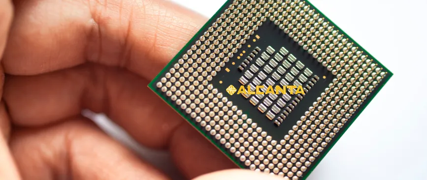
Maximizing Performance: 4-Up FCBGA Substrates
Flip chip technology revolutionized electronic packaging by enabling smaller, faster, and more reliable devices. Unlike traditional wire bonding, flip chip bonding directly connects the chip to the substrate, enhancing electrical performance and reducing signal interference. This method finds extensive applications in microprocessors, memory chips, and high-speed communication devices. The substrate material in flip chip BGA packaging plays a crucial role in providing structural support, thermal dissipation, and electrical connectivity. Selecting the right substrate material ensures optimal performance, reliability, and manufacturability of flip chip BGA packages, making it a critical consideration in electronic design and manufacturing processes.
Flip Chip vs. BGA: Understanding the Differences
Flip chip and Ball Grid Array (BGA) are two popular packaging technologies used in electronic devices, each with its unique characteristics and applications.
Flip Chip Technology:
Flip chip technology involves mounting the semiconductor die face-down onto the substrate or carrier, with the active side of the die facing the substrate. Electrical connections are made through solder bumps deposited on the die’s bonding pads, which are then flipped and aligned with corresponding pads on the substrate. This direct connection minimizes the signal path length, reduces inductance, and enhances electrical performance.
BGA Technology:
Ball Grid Array (BGA) packaging involves mounting the semiconductor die face-up onto the substrate or carrier. Solder balls are attached to the die’s bonding pads, forming an array of connections on the underside of the package. These solder balls are then soldered to corresponding pads on the substrate, providing electrical connections. BGA packages offer high-density interconnects and good thermal performance, making them suitable for various applications.
Contrasting Features:
– Orientation: Flip chip packages have the die mounted face-down, while BGA packages have the die mounted face-up.
– Interconnection Method: Flip chip uses solder bumps for direct connections, while BGA uses solder balls for connections.
– Signal Path Length: Flip chip offers shorter signal paths, reducing signal delay and improving electrical performance.
– Thermal Management: BGA packages typically have better thermal dissipation due to the exposed die, while flip chip packages may require additional thermal management solutions.
– Cost: BGA packages are often more cost-effective for lower pin count applications, while flip chip packages may offer better performance but at a higher cost.
Advantages of Flip Chip BGA (FCBGA) Substrates:
– Enhanced Electrical Performance: FCBGA substrates offer shorter signal paths, reduced inductance, and improved signal integrity compared to traditional wire bonding or BGA packages.
– Higher Density Interconnects: FCBGA substrates can accommodate a higher number of I/Os, enabling the integration of complex electronic systems into smaller form factors.
– Improved Thermal Management: By directly attaching the die to the substrate, FCBGA substrates offer efficient heat dissipation, crucial for high-power applications.
– Reliability: The direct solder connections in FCBGA substrates enhance reliability by reducing the risk of wire bond failures and providing better mechanical stability.
In summary, while both flip chip and BGA packaging technologies have their advantages and limitations, flip chip BGA substrates offer superior electrical performance, higher density interconnects, improved thermal management, and enhanced reliability, making them ideal for a wide range of high-performance electronic applications.
Understanding Flip Chip BGA (FCBGA) Packaging
Definition and Characteristics of FCBGA:
Flip Chip BGA (FCBGA) packaging combines the benefits of flip chip technology with the structural support and ease of assembly provided by Ball Grid Array (BGA) packages. In FCBGA, the semiconductor die is flip-chip bonded onto the substrate, which is then encapsulated with a protective material. The substrate features a grid array of solder balls for external connections, ensuring reliable electrical and mechanical connections between the die and the printed circuit board (PCB). FCBGA packages offer high-density interconnects, excellent electrical performance, and robust mechanical properties, making them suitable for a wide range of applications, including microprocessors, GPUs, and ASICs.
Overview of FCBGA Process Flow:
1. Substrate Preparation: The process begins with the preparation of the substrate, which involves the fabrication of the substrate material (usually laminate or ceramic) into the desired size and shape. The substrate is then coated with a layer of solder mask, leaving exposed pads for die attachment and external connections.
2. Die Attach: The semiconductor die is then attached to the substrate using a die attach material such as epoxy or solder paste. Precision alignment is crucial to ensure accurate placement of the die onto the substrate.
3. Flip Chip Bonding: Once the die is securely attached to the substrate, flip chip bonding is performed. Solder bumps on the die are aligned with corresponding pads on the substrate, and the assembly is subjected to controlled heating, causing the solder bumps to reflow and form electrical connections between the die and the substrate.
4. Encapsulation: After flip chip bonding, the entire assembly is encapsulated with a protective material such as epoxy or molding compound. Encapsulation provides mechanical reinforcement, protects the die and interconnects from external environmental factors, and enhances the overall reliability of the package.
5. Solder Ball Attachment: Finally, solder balls are attached to the underside of the substrate to form the external connections. This process involves applying solder paste or preformed solder balls to the substrate, followed by reflow soldering to attach the balls to the exposed pads.
6. Testing and Inspection: The completed FCBGA packages undergo rigorous testing and inspection processes to ensure quality and reliability. This may include electrical testing, visual inspection, and thermal cycling to simulate real-world operating conditions.
By following these steps, FCBGA packages are manufactured with high precision, reliability, and performance, meeting the demanding requirements of modern electronic devices.
Substrate Material for Flip Chip
Detailed Exploration of Substrate Materials:
Several substrate materials are commonly used in flip chip packaging, each offering different properties and advantages:
1. Laminate Substrates: Made from multiple layers of fiberglass-reinforced epoxy resin, laminate substrates are cost-effective and widely used in flip chip packaging. They offer good dimensional stability, electrical insulation, and ease of fabrication. However, laminate substrates may have limitations in terms of thermal conductivity and coefficient of thermal expansion (CTE) mismatch with the die material.
2. Ceramic Substrates: Ceramic substrates, such as alumina (Al2O3) or aluminum nitride (AlN), offer excellent thermal conductivity, low CTE, and high mechanical strength. They provide superior thermal management capabilities, making them ideal for high-power flip chip applications. Ceramic substrates also exhibit good electrical insulation properties and are suitable for high-frequency applications.
3. Flexible Substrates: Flexible substrates, typically made from polyimide or liquid crystal polymer (LCP), offer flexibility and conformability, making them suitable for applications requiring bendability or stretchability. They are commonly used in flip chip packaging for wearable devices, flexible displays, and medical electronics.
4. Metal Core Substrates: Metal core substrates, such as aluminum or copper, feature a metal layer for enhanced thermal conductivity. They provide efficient heat dissipation and are suitable for high-power flip chip applications where thermal management is critical.
Properties and Requirements of Ideal Substrate Materials:
– Thermal Conductivity: Ideal substrate materials for flip chip applications should have high thermal conductivity to efficiently dissipate heat generated by the semiconductor die.
– Coefficient of Thermal Expansion (CTE): The substrate material’s CTE should closely match that of the semiconductor die to minimize thermal stress and prevent solder joint failures.
– Electrical Insulation: Substrate materials should provide excellent electrical insulation to prevent short circuits and ensure reliable performance.
– Dimensional Stability: Substrates should exhibit good dimensional stability to maintain precise alignment between the die and the substrate, especially during thermal cycling.
– Mechanical Strength: Substrate materials should have sufficient mechanical strength to withstand handling and assembly processes without deformation or damage.
Discussion on the Suitability of Laminate Substrates for FCBGA Packages:
Laminate substrates are commonly used in FCBGA packages due to their cost-effectiveness and ease of fabrication. They offer adequate electrical insulation and dimensional stability for most flip chip applications. However, laminate substrates may have limitations in terms of thermal conductivity, which can impact thermal management in high-power applications. Additionally, CTE mismatch between the laminate substrate and the semiconductor die may require careful design considerations to mitigate thermal stress and ensure reliability. Despite these limitations, laminate substrates remain a popular choice for FCBGA packages in many consumer electronics and automotive applications where cost is a significant factor.
Flip Chip Bonding Material
Explanation of Flip Chip Bonding Materials:
Several materials are commonly used for flip chip bonding, each offering unique properties and advantages:
1. Solder: Solder is a common bonding material used in flip chip packaging due to its low melting point, high electrical conductivity, and ease of reflow. Lead-based solders, such as eutectic solder (63% tin, 37% lead), have traditionally been used for flip chip bonding. However, with the shift towards lead-free manufacturing, alternative solder alloys like SAC (tin-silver-copper) and SnAgCu (tin-silver-copper) are now widely adopted.
2. Conductive Adhesives: Conductive adhesives consist of a polymer matrix filled with conductive particles, such as silver or carbon. They offer lower processing temperatures compared to solder, making them suitable for heat-sensitive components. Conductive adhesives also provide good electrical conductivity and mechanical flexibility.
3. Underfill Materials: Underfill materials are used to fill the gap between the semiconductor die and the substrate after flip chip bonding. They improve mechanical strength, thermal conductivity, and reliability by reducing stress on the solder joints and preventing moisture ingress. Underfill materials are typically epoxy-based and may contain filler particles for enhanced thermal conductivity.
Comparison of Bonding Materials:
– Conductivity: Solder offers the highest electrical conductivity among flip chip bonding materials, making it ideal for high-speed and high-frequency applications. Conductive adhesives also provide good conductivity but may have slightly higher resistivity compared to solder.
– Reliability: Solder joints typically offer excellent reliability, especially when properly designed and processed. Conductive adhesives may have lower reliability compared to solder, particularly under thermal cycling or mechanical stress.
– Thermal Properties: Solder has good thermal conductivity, allowing efficient heat transfer away from the semiconductor die. Underfill materials can further enhance thermal performance by improving heat dissipation and reducing thermal stress on the solder joints.
Importance of Selecting the Right Bonding Material for FCBGA Substrates:
Selecting the appropriate bonding material is crucial for ensuring the performance, reliability, and manufacturability of FCBGA packages. The right bonding material should:
1. Meet Electrical Requirements: The bonding material should provide low electrical resistance to ensure efficient signal transmission and minimize signal loss.
2. Ensure Mechanical Integrity: The bonding material should offer sufficient mechanical strength to withstand thermal cycling, mechanical shock, and vibration encountered during the device’s lifetime.
3. Facilitate Thermal Management: The bonding material should have good thermal conductivity to dissipate heat generated by the semiconductor die, preventing overheating and ensuring long-term reliability.
4. Support Manufacturing Processes: The bonding material should be compatible with the manufacturing processes involved in FCBGA packaging, including die attach, flip chip bonding, and encapsulation.
By carefully evaluating the properties and performance of different bonding materials, engineers can select the most suitable option for specific FCBGA applications, ensuring optimal performance and reliability of electronic devices.
Advantages of 4 Up Flip Chip BGA Substrate
Highlighting the Unique Features and Benefits of 4 Up FCBGA Substrates:
1. Higher Density Interconnects: 4 Up FCBGA substrates allow for the integration of multiple semiconductor dies within a single package, increasing the density of interconnects and enabling the realization of more complex electronic systems in a smaller footprint.
2. Improved Signal Integrity: With multiple dies housed in a single package, 4 Up FCBGA substrates minimize signal propagation delays and reduce signal interference, leading to improved signal integrity and enhanced overall performance of electronic devices.
3. Enhanced Thermal Management: By distributing heat dissipation across multiple dies, 4 Up FCBGA substrates offer superior thermal management capabilities compared to traditional BGA packages. This results in lower operating temperatures, increased reliability, and extended lifespan of electronic components.
4. Cost Efficiency: Despite the higher complexity of 4 Up packaging, FCBGA substrates can achieve cost efficiencies by consolidating multiple components into a single package, reducing assembly and testing costs, and simplifying supply chain logistics.
Increased Efficiency and Scalability Achieved Through 4 Up Packaging:
1. Streamlined Assembly Process: 4 Up FCBGA substrates streamline the assembly process by reducing the number of individual components that need to be mounted and interconnected, leading to shorter assembly times and improved manufacturing efficiency.
2. Scalability: The modular nature of 4 Up packaging allows for easy scalability, enabling manufacturers to customize package configurations based on specific application requirements. This scalability facilitates rapid prototyping, accelerates time-to-market, and enhances product flexibility.
Enhanced Thermal Management and Electrical Performance Compared to Traditional BGA Packages:
1. Improved Thermal Dissipation: Traditional BGA packages may struggle with thermal management due to the concentration of heat in a single die. In contrast, 4 Up FCBGA substrates distribute heat more evenly across multiple dies, reducing thermal hotspots and improving overall thermal dissipation.
2. Optimized Electrical Performance: With shorter signal paths and reduced inductance, 4 Up FCBGA substrates offer optimized electrical performance, resulting in faster data transmission, lower power consumption, and enhanced system reliability compared to traditional BGA packages.
In summary, 4 Up Flip Chip BGA substrates offer a range of unique advantages, including higher density interconnects, improved thermal management, cost efficiency, streamlined assembly processes, scalability, and optimized electrical performance. These benefits make them an attractive choice for a wide range of high-performance electronic applications, from consumer electronics to telecommunications infrastructure.
Applications and Market Trends
Overview of Industries and Applications Benefiting from 4 Up FCBGA Substrates:
1. Telecommunications: 4 Up FCBGA substrates are widely used in telecommunications equipment such as routers, switches, and base stations. These substrates enable high-speed data processing, efficient thermal management, and compact form factors, crucial for meeting the demands of 5G networks and beyond.
2. Data Centers: With the increasing demand for data storage and processing capabilities, 4 Up FCBGA substrates play a vital role in data center infrastructure. They enable the integration of multiple processing units within a single package, improving computing power, energy efficiency, and scalability.
3. Automotive Electronics: Automotive electronics require high reliability, robust thermal management, and compact designs to withstand harsh environmental conditions. 4 Up FCBGA substrates are used in automotive control units, infotainment systems, and advanced driver assistance systems (ADAS) to meet these requirements while offering enhanced performance and reliability.
4. Consumer Electronics: From smartphones and tablets to gaming consoles and wearables, consumer electronics benefit from the compact size, improved thermal management, and high performance offered by 4 Up FCBGA substrates. These substrates enable manufacturers to pack more functionality into smaller devices without compromising on performance or reliability.
Analysis of Current Market Trends and Future Growth Projections for FCBGA Technology:
1. Increasing Demand for High-Performance Computing: The growing demand for high-performance computing (HPC) applications, including artificial intelligence (AI), machine learning (ML), and big data analytics, is driving the adoption of FCBGA technology. As these applications require faster data processing, lower power consumption, and improved thermal management, 4 Up FCBGA substrates are expected to see significant growth in the coming years.
2. Expansion of 5G Networks: The rollout of 5G networks is driving demand for advanced telecommunications equipment capable of handling increased data traffic and supporting low-latency applications. FCBGA substrates enable the development of compact, high-performance equipment essential for 5G infrastructure, including base stations, small cells, and network switches.
3. Automotive Industry Trends: The automotive industry is undergoing a transformation with the rise of electric vehicles (EVs), autonomous driving technologies, and connected car systems. FCBGA substrates are integral to the development of automotive electronics, providing the performance, reliability, and thermal management required for next-generation vehicles.
4. Emerging Applications in IoT and Edge Computing: The proliferation of Internet of Things (IoT) devices and edge computing platforms is creating new opportunities for FCBGA technology. These substrates enable the development of compact, energy-efficient devices capable of processing and analyzing data at the edge of the network, enhancing real-time decision-making and reducing latency.
Case Studies or Examples Demonstrating the Success of 4 Up FCBGA Substrates in Real-World Applications:
1. Networking Equipment: A leading networking equipment manufacturer implemented 4 Up FCBGA substrates in their high-performance routers and switches, achieving significant improvements in data processing speed, energy efficiency, and space utilization.
2. Automotive Control Units: A major automotive OEM incorporated 4 Up FCBGA substrates in their advanced control units for electric vehicles, enhancing thermal management and reliability while reducing the overall footprint of the system.
3. Cloud Computing Servers: A leading cloud computing provider deployed servers equipped with 4 Up FCBGA substrates in their data centers, resulting in higher computing density, lower power consumption, and improved overall performance.
4. Wearable Devices: A wearable technology company utilized 4 Up FCBGA substrates in their smartwatches and fitness trackers, achieving a compact design, longer battery life, and enhanced processing capabilities, catering to the demands of active consumers.
These case studies demonstrate the successful implementation of 4 Up FCBGA substrates across various industries and applications, highlighting their versatility, performance, and reliability in real-world scenarios. As technological advancements continue and demand for high-performance electronic devices grows, FCBGA technology is poised to play a pivotal role in shaping the future of electronics.
FAQs about 4 up flip chip bga substrate
The substrate material for flip chip can vary depending on the specific application and requirements. Common substrate materials for flip chip packaging include laminate, ceramic, and metal core substrates.
Flip chip and BGA (Ball Grid Array) are two different packaging technologies. While they both involve mounting semiconductor dies onto substrates, they differ in the orientation of the die and the method of interconnection. In flip chip packaging, the die is mounted face-down on the substrate, and electrical connections are made through solder bumps. In BGA packaging, the die is typically mounted face-up, and electrical connections are made through solder balls on the underside of the package.
The material used for flip chip bonding is typically solder. Solder bumps are deposited on the bonding pads of the semiconductor die, and when heated, they reflow to form electrical connections with corresponding pads on the substrate.
The substrate of a BGA (Ball Grid Array) package is typically made from materials such as laminate, ceramic, or organic substrates. These substrates provide structural support and electrical connections for the semiconductor die and facilitate the attachment of solder balls for external connections.

