
The Role of Leadframes DFN in Semiconductor Packaging
In the semiconductor industry, packaging plays a crucial role in protecting integrated circuits (ICs) and ensuring their functionality within electronic systems. Proper packaging not only safeguards the delicate ICs but also facilitates their integration with other components. One essential part of semiconductor packaging is the Leadframes DFN, which serves as the foundation for the connections between the chip and external devices. Leadframes are metal structures that help guide electrical signals from the IC to the board, offering both mechanical support and electrical conductivity. Among various packaging options, the DFN (Dual Flat No-lead) and QFN (Quad Flat No-lead) packages have gained significant popularity due to their compact size, high performance, and improved thermal dissipation. These packaging types, made possible by advanced leadframe technology, are commonly used in consumer electronics, automotive, and telecommunications, where space and reliability are paramount.
What is a Leadframe in Leadframes DFN Packaging?
A Leadframe is a critical component in semiconductor packaging, serving as the metal framework that supports the chip and connects it to external electronic systems. In the context of Leadframes DFN packaging, the leadframe acts as a bridge for the electrical connections between the integrated circuit (IC) and the circuit board, ensuring that signals and power flow efficiently. This structure enables the proper functioning of the semiconductor by providing both mechanical support and electrical conduction.
The primary function of a leadframe is to provide a reliable interface between the semiconductor chip and the external environment. It connects the chip’s bond pads to the external pins or leads, which are used to interface with other components or devices. These leads typically form the path through which electrical signals are transmitted to and from the chip, making the leadframe a vital element in the overall performance of the package.
Leadframes are often made from copper or copper alloys due to their excellent conductivity, corrosion resistance, and cost-effectiveness. In Leadframes DFN packaging, these materials are carefully chosen to ensure optimal performance, durability, and thermal management. Copper is particularly favored for its high thermal conductivity, which is crucial for managing the heat generated by high-power chips. Alloys such as copper-tungsten or copper-nickel may also be used in specialized applications, offering enhanced strength and thermal properties.
Leadframes in Leadframes DFN packaging are indispensable for creating robust electrical connections and ensuring that the semiconductor package performs reliably in various applications, from consumer electronics to automotive systems.
Process of Leadframe Manufacturing in Leadframes DFN Packaging
The manufacturing process of leadframes, particularly in Leadframes DFN packaging, involves several highly precise and intricate steps to ensure the quality and reliability of the final product. These processes include stamping, etching, and plating, each of which plays a crucial role in shaping the leadframe and preparing it for integration with semiconductor chips.
-
Stamping
The first step in leadframe manufacturing is stamping, where a flat metal sheet, typically made of copper or copper alloys, is fed into a press machine. The machine then punches or stamps the material into the desired leadframe shape. This process creates the basic structure of the leadframe, including the leads that will connect the semiconductor chip to external components. Stamping ensures that the leadframe has the correct dimensions and spacing for the IC’s bonding pads. -
Etching
After the leadframe has been stamped, etching is used to refine the structure further. In this step, specific patterns are etched onto the leadframe to define areas where the chip will be placed and where electrical connections will occur. Etching is typically done using a chemical solution that removes unwanted material, leaving behind the intricate design necessary for the electrical and mechanical properties of the package. The etching process is especially critical for Leadframes DFN, as the precise alignment of the leads ensures reliable electrical connections and thermal dissipation. -
Plating
Once the leadframe has been etched, it undergoes plating to improve its conductivity, corrosion resistance, and solderability. In most cases, a thin layer of gold, silver, or tin is applied over the copper or alloy-based frame. This plating helps to ensure that the leads of the Leadframes DFN package can withstand the rigors of soldering during assembly and continue to maintain a reliable connection throughout the device’s lifecycle. Plating also enhances the leadframe’s resistance to oxidation, ensuring long-term durability in various environmental conditions. -
Assembly and Testing
After the leadframe has been shaped and plated, it is ready for assembly with the semiconductor chip. The chip is wire-bonded or flip-chipped onto the leadframe, and the connections are sealed with molding compounds. Finally, the assembled Leadframes DFN package undergoes rigorous testing to ensure that all electrical connections are intact and that the device meets performance specifications.
The precision in each step of the leadframe manufacturing process is paramount to ensuring the Leadframes DFN package’s high performance and reliability. Any slight deviation in dimensions or alignment can lead to failures in electrical connections or thermal management, which could compromise the performance of the semiconductor device. Therefore, manufacturers use advanced technology and quality control measures at every stage to achieve the high standards required for modern electronics.
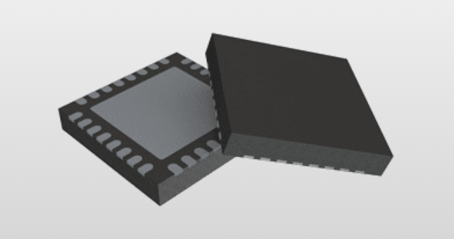
What is DFN (Dual Flat No-lead) Package in Leadframes DFN Packaging?
The DFN (Dual Flat No-lead) package is a popular semiconductor packaging option known for its compact design and excellent thermal and electrical performance. Unlike traditional packages that feature leads extending from all sides, the DFN package has leads on only two sides, which are typically underneath the package. This structure contributes to its space-saving, low-profile form factor, making it ideal for modern, miniaturized electronic devices where space is limited.
Structure of a DFN Package
The DFN package consists of a flat, rectangular body with electrical leads placed on the bottom surface, which connect directly to the PCB (Printed Circuit Board). These leads are typically formed as pads that are directly soldered to the PCB, making the connections less prone to mechanical stress compared to traditional leaded packages. This design allows the Leadframes DFN package to have a low-profile height while still maintaining high functionality. The chip within the package is typically wire-bonded to the leadframe, with the leadframe itself acting as the pathway for electrical signals between the chip and the external circuitry.
Comparison Between DFN and Other Package Types (e.g., QFN)
While both DFN and QFN (Quad Flat No-lead) packages fall under the “no-lead” category, they differ in a few important ways:
-
Lead Placement: The most obvious difference is in the placement of the leads. In a QFN package, the leads are located on all four sides of the package, whereas in a DFN package, the leads are positioned only on two sides, generally underneath the package. This makes DFN packages more compact and ideal for devices with size constraints.
-
Size and Footprint: Leadframes DFN packages have a smaller footprint compared to QFN packages, making them ideal for applications where board space is at a premium. The smaller footprint of DFN also provides better flexibility in board layout, allowing for more efficient use of space in tightly packed electronic devices.
-
Thermal Performance: Both DFN and QFN packages offer good thermal performance, but DFN packages typically provide superior heat dissipation. The bottom-mounted leads and the flat structure of the DFN package allow for more efficient heat flow directly to the PCB, improving thermal management. This makes DFN packages particularly well-suited for power-sensitive applications where managing heat is a critical factor.
Benefits of DFN Packages
-
Smaller Footprint: The DFN (Dual Flat No-lead) package is significantly smaller than traditional packages such as the standard QFN or through-hole components. This smaller footprint is a huge advantage for compact consumer electronics, portable devices, and wearables, where minimizing the size of each component is essential.
-
Better Thermal Performance: One of the major advantages of Leadframes DFN packaging is its superior thermal management. The flat, lead-on-bottom design allows heat to dissipate more efficiently through the PCB, which is particularly important in high-power applications. The efficient thermal management helps prevent overheating and ensures the semiconductor operates within its safe temperature range.
-
Increased Reliability: The design of the DFN package, especially in the context of Leadframes DFN, provides enhanced mechanical stability. The leads are protected by the body of the package, reducing the risk of damage during handling or assembly. Furthermore, the direct contact between the leads and the PCB ensures a robust electrical connection, minimizing the chances of failure due to poor contact or mechanical stress.
-
Improved Electrical Performance: With the leads located directly underneath the package, the electrical connections are typically shorter, which reduces the overall inductance and resistance in the package. This translates to better electrical performance, particularly in high-speed and high-frequency applications.
Leadframes DFN packages are an excellent choice for applications requiring a compact, efficient, and reliable packaging solution. Their smaller footprint, superior thermal performance, and enhanced reliability make them ideal for use in advanced electronic devices, from smartphones to automotive systems.
DFN vs. QFN Package in Leadframes DFN Packaging
When choosing between DFN (Dual Flat No-lead) and QFN (Quad Flat No-lead) packages, understanding their design differences, applications, and performance characteristics is essential. While both are no-lead package types offering space-efficient and high-performance solutions, they each have distinct advantages and are suited to different applications. Let’s explore the key factors that differentiate these two package types.
Design Differences: Leadframe Configuration
The most noticeable design difference between Leadframes DFN and QFN packages lies in the placement of the leads:
-
DFN Package: In a DFN (Dual Flat No-lead) package, the leads are located only on two sides of the package, typically underneath the package body. This configuration allows for a more compact design with a smaller footprint, which is particularly useful when space is limited. The leads are arranged as flat pads directly connected to the PCB, offering a simpler design with fewer points of connection.
-
QFN Package: In contrast, a QFN (Quad Flat No-lead) package has leads on all four sides of the package. The leadframe in a QFN package provides a larger area for the electrical connections, which can accommodate higher current loads and more robust mechanical bonding. While the QFN package offers the same bottom-pad contact with the PCB, its four-sided leads make it more suitable for applications where additional mechanical strength and electrical capacity are needed.
Applications: When to Use DFN vs. QFN
Choosing between Leadframes DFN and QFN packages often depends on specific application requirements, such as size constraints, power requirements, and thermal performance:
-
DFN Package: Leadframes DFN packages are ideal for applications where a smaller footprint is essential. These packages are commonly used in portable electronic devices such as smartphones, wearables, and compact sensors, where every millimeter of board space is valuable. The compact nature of DFN packages also makes them a good fit for low-to-moderate power applications that do not require the higher mechanical or electrical strength provided by QFN packages.
-
QFN Package: On the other hand, QFN packages are better suited for higher power applications or designs where a larger leadframe is required for enhanced current-carrying capacity. Their four-sided leads make them more robust for devices that require additional mechanical support, such as power management ICs, automotive electronics, and some communications equipment. QFN packages also excel in applications that require improved heat dissipation and higher reliability in demanding environments.
Performance: Comparing Heat Dissipation, Current Carrying Capabilities, and Mechanical Strength
When it comes to performance, both Leadframes DFN and QFN packages offer excellent thermal and electrical properties, but they differ in certain aspects that impact their suitability for specific tasks:
-
Heat Dissipation: Heat management is a crucial factor in modern electronics, and both package types offer excellent thermal performance. However, the Leadframes DFN package typically provides better heat dissipation due to its bottom-mount lead design. The heat generated by the semiconductor can more efficiently travel through the PCB, allowing for lower junction temperatures. This makes DFN packages especially useful in applications that require efficient thermal management in a compact design, such as mobile devices and portable electronics.
In comparison, QFN packages also offer good thermal performance but may have a slightly higher thermal resistance due to the larger leadframe area. The four sides allow for a larger surface area for heat flow, but the presence of more leads can sometimes create additional thermal barriers, making the heat dissipation slightly less efficient than in DFN packages.
-
Current Carrying Capabilities: QFN packages generally offer better current carrying capacity than Leadframes DFN packages due to the larger number of leads and the more robust structure of the QFN leadframe. The four leads provide multiple pathways for current to flow, which is beneficial for applications requiring higher power or higher current density. This makes QFN packages ideal for power management ICs, motor controllers, and other high-current applications.
Conversely, the Leadframes DFN package’s two-sided leads are sufficient for lower to moderate current applications. The compact size and simpler design make it a preferred choice for low-power electronics, where the high current capacity of a QFN is not necessary.
-
Mechanical Strength: QFN packages tend to offer better mechanical strength compared to Leadframes DFN due to their four-sided leadframe configuration. The more leads provide additional support, making QFN packages better suited for harsh environments where mechanical stress is a concern, such as automotive and industrial applications.
Leadframes DFN, with leads on only two sides, offer adequate mechanical strength for compact, low-stress applications but are generally not as robust as QFN packages in high-vibration or high-stress environments.
Leadframes DFN and QFN packages each have unique advantages depending on the application. Leadframes DFN packages offer a smaller footprint, superior thermal dissipation, and are ideal for low-to-moderate power applications in compact devices. On the other hand, QFN packages are better suited for higher-power, high-current, and mechanical strength-demanding applications, such as power management systems and automotive electronics. Choosing between these two package types depends on the specific needs of the design, including thermal performance, size constraints, and the amount of current the device must handle.
Caplinq’s Role in Leadframes DFN Technology
Caplinq is a leading supplier of materials and components that play a crucial role in the semiconductor packaging industry, particularly in the design and manufacturing of Leadframes DFN and other advanced package types. With its extensive expertise in providing customized solutions, Caplinq supports companies that require high-performance packaging for their semiconductor products. By offering a range of specialized leadframe solutions, Caplinq enables engineers to create more efficient, reliable, and cost-effective packages for a wide variety of applications.
Caplinq’s Products for Semiconductor Packaging
Caplinq provides a comprehensive portfolio of materials and products designed to support the unique needs of semiconductor packaging, with a strong emphasis on Leadframes DFN technology. The company offers not only the raw materials for leadframes but also the necessary tools and processes for fabricating DFN and QFN packages. This includes high-quality, customizable etched leadframes that are integral to the performance and reliability of modern semiconductor packages.
One of Caplinq’s key offerings is LinqAlloy, a line of customizable etched leadframes specifically designed for Leadframes DFN and QFN packages. These leadframes are etched to precise specifications, offering better control over the material properties, geometry, and design flexibility. By using these etched leadframes, semiconductor manufacturers can create packages that meet specific performance, size, and thermal management requirements. The company also provides an array of additional materials for use in packaging, including molding compounds and bonding wires, which further enhance the overall quality and functionality of the final product.
Customizable Etched Leadframes for DFN and QFN Packages
One of Caplinq’s standout offerings for Leadframes DFN technology is the ability to produce customizable etched leadframes. These etched leadframes are manufactured to the highest standards of precision and reliability, ensuring that they meet the exact specifications required for DFN and QFN packages. Customizable leadframes allow for greater flexibility in terms of size, material composition, and design, making them suitable for a wide range of applications.
For Leadframes DFN packages, Caplinq’s etched leadframes are designed to optimize the small, compact footprint that is characteristic of DFN packages, ensuring that the leads provide excellent electrical conductivity while also supporting efficient thermal management. The precision with which these leadframes are etched ensures that the design maintains optimal contact with the PCB and enhances the overall performance of the packaged semiconductor device.
Link to Caplinq’s Leadframe Solutions
Caplinq’s extensive range of leadframe solutions, including those designed specifically for Leadframes DFN packaging, can be explored further on their official website. Whether you’re looking for customizable etched leadframes, advanced materials, or comprehensive semiconductor packaging solutions, Caplinq provides the expertise and tools needed to bring high-performance devices to market.
To learn more about Caplinq’s offerings for Leadframes DFN and other packaging solutions, visit their dedicated leadframe page: Caplinq Leadframes.
Caplinq’s commitment to innovation and quality in the semiconductor packaging industry ensures that their customers have access to the best possible materials and solutions for creating reliable, efficient, and high-performance Leadframes DFN packages.
Advantages of DFN and QFN Packages in Leadframes DFN Technology
DFN (Dual Flat No-lead) and QFN (Quad Flat No-lead) packages, when used in Leadframes DFN technology, offer a range of significant advantages that make them highly desirable for a wide array of semiconductor applications. These packages provide a compact design, enhanced electrical performance, and superior thermal management, making them ideal for modern electronic devices that demand high efficiency and reliability.
Compact Design: Small Form Factor Ideal for Portable Devices
One of the most notable benefits of Leadframes DFN and QFN packages is their compact form factor, which is essential for today’s miniaturized electronic devices. Leadframes DFN packages, in particular, have a small, low-profile design that is ideal for portable and wearable devices. This small size enables manufacturers to create highly integrated products that are lightweight and easy to incorporate into tight spaces, making them perfect for smartphones, tablets, smartwatches, hearing aids, and other consumer electronics where space is a premium.
The two-sided lead design of DFN packages (versus four-sided in QFN packages) allows for a highly compact layout, offering a substantial reduction in height compared to traditional leaded packages. This smaller footprint results in more efficient use of the available PCB space, enabling other components to fit into the design and improving overall product performance and functionality.
Enhanced Electrical Performance: Low Inductance and High-Speed Performance
Both Leadframes DFN and QFN packages are designed to provide superior electrical performance, especially in high-speed or high-frequency applications. The direct contact between the leads and the PCB in Leadframes DFN packaging offers a significantly lower inductance than conventional leaded packages, which is critical for high-speed signal transmission. The leads are shorter and closer to the PCB, reducing signal loss and making DFN packages ideal for applications where signal integrity is paramount, such as in communication devices, automotive systems, and networking equipment.
The absence of traditional leads and the bottom-mount connection of Leadframes DFN packages result in reduced parasitic inductance, making them more suitable for high-frequency applications. As a result, DFN packages ensure faster data transmission and better high-speed performance, meeting the demands of modern electronic devices that require high-speed, low-latency performance.
Thermal Performance: Better Heat Dissipation Compared to Other Package Types
In addition to their compact size and electrical benefits, Leadframes DFN and QFN packages offer excellent thermal management properties, a crucial factor in ensuring the reliable operation of semiconductor devices, particularly those that generate significant heat. The Leadframes DFN package, with its bottom-lead design, enhances heat dissipation directly through the PCB, offering better heat flow and lowering the overall junction temperature of the chip.
Because the leads in Leadframes DFN packages are in direct contact with the PCB, the thermal resistance is lower, which means that heat is more efficiently transferred away from the device. This efficient heat dissipation helps prevent overheating and enhances the long-term reliability of the semiconductor device. Similarly, QFN packages also benefit from their no-lead design and bottom-side leads, which provide enhanced thermal conduction, although the larger size and four leads may result in slightly less efficient heat dissipation compared to DFN packages in certain applications.
Both package types are more thermally effective than traditional packages, such as the Through-Hole and Surface-Mount Devices (SMD), which often require additional components like heat sinks or thermal vias. The Leadframes DFN package, in particular, is highly effective in space-constrained applications where passive cooling options are limited.
The Leadframes DFN package offers a range of advantages, including its compact design, superior electrical performance, and exceptional thermal management. These benefits make it an ideal choice for modern electronic devices, particularly those requiring miniaturization, high-speed performance, and efficient heat dissipation. Whether you are designing portable consumer electronics, automotive systems, or other high-performance applications, Leadframes DFN and QFN packages deliver the reliability and efficiency needed to meet the demanding requirements of today’s technology landscape.
Applications of DFN and QFN Packages in Leadframes DFN Technology
Leadframes DFN and QFN packages are widely used in a variety of industries due to their small form factor, excellent thermal management, and high-performance capabilities. These packages are designed to meet the growing demands of modern electronics, making them ideal for applications across consumer electronics, automotive, telecommunications, industrial equipment, and more. Let’s explore some of the key industries and devices that benefit from Leadframes DFN and QFN packages.
Common Industries Using DFN and QFN Packages
-
Consumer Electronics: The consumer electronics industry is one of the primary users of Leadframes DFN and QFN packages, especially due to the trend toward smaller, thinner, and more powerful devices. Smartphones, wearables, tablets, and laptops often utilize DFN and QFN packages to accommodate their compact designs while maintaining excellent performance. The need for high-speed performance, low power consumption, and efficient thermal management makes Leadframes DFN a perfect fit for these devices.
- Example Devices: Smartphone processors, Bluetooth chips, accelerometers, gyroscopes, and touch sensors.
-
Automotive: The automotive industry relies on advanced electronics for everything from infotainment systems to safety features, such as airbags, anti-lock braking systems (ABS), and electronic stability control (ESC). DFN and QFN packages are commonly used in automotive applications because they offer a balance of mechanical robustness and performance under harsh conditions, such as extreme temperatures and vibrations.
- Example Devices: Power management ICs, temperature sensors, pressure sensors, LED drivers for automotive lighting systems, and engine control units (ECUs).
-
Telecommunications: As the demand for high-speed communication continues to grow, Leadframes DFN and QFN packages are integral to the telecom industry. These packages support the development of smaller, more efficient telecom equipment, such as base stations, routers, and optical communication systems. Their low inductance and high-frequency capabilities make them ideal for handling the high-speed data transfer requirements of telecommunications equipment.
- Example Devices: RF power amplifiers, data converters, transceivers, and antennas used in 4G/5G infrastructure.
-
Industrial Equipment: In industrial applications, electronics are used to control machinery, monitor systems, and improve operational efficiency. Leadframes DFN and QFN packages provide the necessary reliability and performance needed for these demanding environments. These packages are commonly found in sensors, controllers, and power management systems used in automation, robotics, and other industrial equipment.
- Example Devices: Motor controllers, temperature sensors, proximity sensors, and voltage regulators used in industrial robots and control systems.
-
Medical Devices: The medical device industry also benefits from the small size, low power consumption, and high reliability offered by Leadframes DFN and QFN packages. These packages are ideal for implantable devices, diagnostic equipment, and wearable health monitors, where precision, reliability, and size are critical factors.
- Example Devices: ECG monitors, hearing aids, glucose sensors, and wearable fitness trackers.
Examples of Devices That Use Leadframes DFN and QFN Packages
-
Sensors: Many types of sensors used in modern electronics, including temperature, pressure, motion, and proximity sensors, utilize Leadframes DFN and QFN packages. The compact design of DFN packages makes them perfect for applications where space is limited, such as in mobile phones or IoT (Internet of Things) devices. These sensors are used to collect and transmit data, making them essential in consumer electronics, automotive, and industrial systems.
- Example Devices: Environmental sensors, accelerometers, gyroscope sensors, and proximity sensors for wearables.
-
Integrated Circuits (ICs): ICs in Leadframes DFN and QFN packages are common in a wide range of applications, from simple consumer electronics to complex industrial control systems. These ICs include processors, memory modules, voltage regulators, and power management ICs. Their small size and high performance allow manufacturers to integrate more functions into a smaller device.
- Example Devices: Power management ICs, voltage regulators, microcontrollers, and communication chips.
-
LED Drivers: Leadframes DFN and QFN packages are particularly beneficial in the LED industry, where efficient thermal management is essential for high-power LEDs used in lighting applications. The excellent heat dissipation properties of these packages ensure the longevity and performance of LED drivers. These drivers are critical for controlling the current and voltage supplied to LEDs, making DFN and QFN packages highly suitable for such applications.
- Example Devices: LED drivers used in automotive lighting, street lights, and indoor/outdoor lighting systems.
-
Power Management: Power management ICs are essential components in most electronic devices, responsible for regulating and distributing power to various parts of the system. Leadframes DFN and QFN packages are widely used for these ICs due to their ability to handle higher currents and provide efficient thermal management.
- Example Devices: DC-DC converters, battery management systems, and power controllers for mobile phones, laptops, and portable devices.
Leadframes DFN and QFN packages are integral to a wide range of industries and applications. From consumer electronics and automotive systems to telecommunications and industrial equipment, these packages offer exceptional benefits in terms of compact design, electrical performance, and thermal management. The use of DFN and QFN packages continues to grow as devices become more compact, energy-efficient, and powerful. Whether it’s in sensors, ICs, LED drivers, or power management solutions, Leadframes DFN technology enables the creation of reliable and high-performance electronic devices across diverse markets.
DFN vs. QFN Assembly in Leadframes DFN Technology
The assembly process for Leadframes DFN and QFN packages involves several key considerations to ensure that the components are efficiently and accurately assembled. Both DFN and QFN packages, due to their unique designs and configurations, require specific techniques to ensure strong electrical connections, proper heat dissipation, and reliable performance throughout their lifecycle. Understanding the differences in their assembly process is crucial for manufacturers to select the right approach and ensure high-quality products.
Key Considerations in the Assembly Process for Both DFN and QFN Packages
-
Lead Configuration and Placement: One of the primary considerations when assembling Leadframes DFN and QFN packages is the lead configuration. DFN packages feature leads on only two sides of the package, which results in a simpler soldering process compared to QFN packages, which have leads on four sides. The two-lead configuration of DFN packages allows for easier alignment during the attachment process, while the four-sided leads in QFN packages require more precise placement and positioning, especially when using automated equipment.
-
Soldering Challenges: Both DFN and QFN packages require accurate soldering techniques to ensure proper electrical connections and mechanical strength. Leadframes DFN packages, with their bottom-side leads, often use reflow soldering methods. During reflow soldering, the solder paste is applied to the PCB, and the package is placed onto the paste. Heat is then applied to melt the solder and create solid connections. For Leadframes DFN, the key challenge is ensuring that solder reflows evenly across the leads and that there is no excessive bridging, especially in the tight spacing between the leads and the PCB.
QFN packages, due to their larger lead area and four-lead configuration, often require more careful soldering to ensure that all leads are properly soldered without voids, which can impair electrical conductivity and thermal dissipation. Both DFN and QFN packages benefit from a reliable solder paste that ensures strong joints and low resistance connections, but DFN packages may be slightly easier to assemble due to their smaller footprint.
Soldering and Attachment Methods
-
Reflow Soldering: Both Leadframes DFN and QFN packages typically utilize reflow soldering as the primary attachment method. This process involves the application of solder paste to the PCB pads, followed by the placement of the package onto the paste. The entire assembly is then heated to a temperature where the solder paste melts and forms strong joints between the leads and the PCB. After cooling, the solder solidifies, securing the package in place.
For Leadframes DFN, the reflow soldering process is often simpler because the leads are on only two sides, reducing the risk of solder bridging or misalignment during the process. However, care must still be taken to avoid issues such as voiding under the leads, which could impact the thermal and electrical performance of the device.
QFN packages, being larger and having leads on four sides, may require additional steps or more meticulous care during reflow soldering to ensure that the leads all receive the right amount of solder and that the package is securely attached without defects such as cold solder joints or excessive solder balls.
-
Conductive Adhesives: In some cases, especially when reflow soldering is not feasible, conductive adhesives may be used as an alternative method for attaching DFN and QFN packages to the PCB. This method involves applying a conductive adhesive in the place of solder paste and using heat to cure the adhesive. While this approach can provide a strong bond, it may not be as efficient in terms of heat dissipation compared to traditional soldering methods.
Compatibility with Automated Assembly and Testing Equipment
-
Automated Assembly: Leadframes DFN and QFN packages are both highly compatible with automated assembly equipment, which is essential for high-volume production. These packages are designed to be handled by pick-and-place machines that can quickly and precisely place the components onto the PCB. The automated process ensures that the components are placed accurately and consistently, reducing the risk of human error and improving production efficiency.
DFN packages, with their two-lead configuration, are easier to handle and align compared to QFN packages. The leads on DFN packages are often positioned along the edges, making them easier for the pick-and-place machines to pick up and place onto the PCB. The smaller size and reduced number of leads contribute to more streamlined assembly, especially in high-density applications.
QFN packages, with their four leads, may require slightly more complex handling. The alignment of these packages requires more precise equipment to ensure that the leads match the PCB pads correctly during the placement process. Despite this, QFN packages are also highly compatible with automated assembly systems, and advancements in machine vision and alignment technology have made handling these packages more efficient.
-
Automated Testing: Once the Leadframes DFN and QFN packages are assembled, they undergo automated testing to verify the functionality and reliability of the connections. Automated optical inspection (AOI) is commonly used to detect issues such as solder bridges, misaligned components, and insufficient solder joints. For DFN packages, which have leads underneath the package, testing may involve x-ray inspection to detect voids or issues under the leads.
QFN packages, with their four-sided leads, are also tested using AOI or x-ray systems. However, because QFN packages typically have a larger footprint and more leads, testing systems are designed to accommodate these differences and ensure that all connections meet quality standards. These automated testing methods ensure that any defects are identified early in the manufacturing process, improving yield and product quality.
The assembly process for Leadframes DFN and QFN packages involves critical steps such as precise soldering, the use of reflow soldering techniques, and compatibility with automated assembly and testing systems. While DFN packages may be slightly easier to handle and assemble due to their smaller lead count and compact form factor, both package types are highly compatible with modern automated manufacturing techniques. The challenges and benefits of assembling Leadframes DFN and QFN packages must be carefully considered to ensure the production of high-quality, reliable semiconductor devices.
Leadframe Materials: Options and Customization in Leadframes DFN Technology
The materials used in the production of Leadframes DFN and other semiconductor packages are crucial for ensuring optimal performance, durability, and reliability. Leadframes DFN packages require high-quality materials to maintain strong electrical connections, excellent heat dissipation, and long-term functionality under various operating conditions. Different materials offer unique properties that cater to diverse packaging needs, and manufacturers can often customize these materials to meet the specific requirements of each application.
Overview of Materials Used in Leadframes DFN (e.g., LinqAlloy Etched Leadframes)
The most common materials used for Leadframes DFN are copper and its alloys, with variations such as copper alloy and LinqAlloy etched leadframes. Each material provides distinct benefits, making them suitable for different types of semiconductor packages.
-
Copper: Copper is widely used in the production of Leadframes DFN due to its excellent electrical conductivity and thermal properties. Copper leadframes offer low resistance, which ensures efficient electrical signal transmission and reduces power loss. Additionally, copper provides superior thermal dissipation, which is essential for managing the heat generated by high-performance semiconductor devices.
- Advantages: High electrical conductivity, good heat dissipation, cost-effective.
- Considerations: Prone to oxidation, requiring protective coatings or plating for enhanced durability.
-
Copper Alloys: Copper alloys, such as copper-tungsten or copper-phosphorus, are also used to manufacture Leadframes DFN packages. These alloys improve the mechanical strength and resistance to corrosion, which is important for maintaining long-term reliability in demanding environments. Copper alloys can also offer improved resistance to stress, which is essential for preventing mechanical failures during thermal cycling or vibrations.
- Advantages: Enhanced mechanical strength, better corrosion resistance, improved fatigue resistance.
- Considerations: More expensive than pure copper.
-
LinqAlloy Etched Leadframes: LinqAlloy is a specialized material that combines the benefits of copper with additional enhancements for use in Leadframes DFN and other advanced semiconductor packages. LinqAlloy etched leadframes are designed for use in high-performance applications, offering superior thermal management, electrical performance, and corrosion resistance. The etching process ensures that the leadframes have precise dimensions, which is crucial for the small and intricate designs of DFN packages.
- Advantages: High thermal and electrical performance, precise etching for small-form factor designs, better mechanical properties for high-reliability applications.
- Considerations: Customization options can increase production costs.
Customizable Solutions for Unique Packaging Requirements
Customization is a key aspect of the materials used in Leadframes DFN technology, as each application may have specific requirements in terms of electrical, mechanical, and thermal performance. Manufacturers like Caplinq provide a wide range of options for Leadframes DFN packages, allowing for tailored solutions based on customer needs.
-
Etching and Forming: Custom etching and forming techniques enable manufacturers to produce leadframes with specific shapes, sizes, and lead configurations. This is particularly useful for DFN packages, where the precise arrangement of leads and the overall size of the frame are critical. The customization process ensures that each leadframe is optimized for the exact specifications of the semiconductor device.
-
Plating and Coatings: Leadframes DFN often require specialized plating or coating to protect against corrosion and improve solderability. Gold, silver, and palladium are common materials used for plating leadframes. Custom coatings can also enhance thermal performance or prevent damage during the assembly process.
- Example: Caplinq’s LinqAlloy etched leadframes can be customized with various plating options to meet the specific electrical and thermal requirements of the device, ensuring optimal performance and longevity.
-
High-Performance Materials: For applications with more demanding performance requirements, such as high-speed circuits, automotive, or aerospace electronics, Leadframes DFN can be customized with high-performance materials that offer greater resistance to thermal stress, better conductivity, and enhanced mechanical strength. These materials ensure that DFN packages can handle the extreme conditions often found in these industries.
How Caplinq and Other Suppliers Offer Specialized Materials for High-Performance Needs
Caplinq and other suppliers are at the forefront of offering specialized materials designed to meet the exacting standards required for Leadframes DFN packages. By providing custom solutions, they enable manufacturers to optimize the performance, reliability, and cost-effectiveness of their products.
-
Caplinq’s LinqAlloy Etched Leadframes: Caplinq offers LinqAlloy etched leadframes, which provide superior thermal and electrical performance, tailored to the needs of DFN and QFN packages. These leadframes are customizable to meet specific packaging requirements, such as reduced size, increased strength, and enhanced conductivity. The etched process ensures high precision, which is especially critical for the tight tolerances found in Leadframes DFN packages.
- Customization Options: Caplinq offers a variety of materials and finishes, such as gold or palladium plating, to optimize the leadframe for different applications. Whether the need is for improved solderability, higher heat dissipation, or greater mechanical strength, Caplinq’s solutions can be tailored to meet those requirements.
-
Collaborative Design and Material Selection: Suppliers like Caplinq work closely with customers to understand their unique needs and offer collaborative design solutions. By using advanced materials, such as high-performance copper alloys or specialized etched leadframes, Caplinq ensures that Leadframes DFN packages perform optimally in their respective applications.
- Example: For a high-speed telecommunications application, Caplinq can provide customized Leadframes DFN packages with enhanced thermal dissipation and low inductance to support the high-frequency requirements of telecom equipment.
-
Other Suppliers: In addition to Caplinq, other suppliers also offer specialized materials for Leadframes DFN and QFN packages. These suppliers focus on providing materials that offer improved mechanical properties, greater reliability under extreme conditions, and better electrical performance. For instance, suppliers might offer materials such as copper-nickel or silver-plated copper for applications requiring enhanced corrosion resistance or better electrical conductivity.
The materials used in Leadframes DFN technology play a critical role in ensuring the performance, reliability, and durability of semiconductor packages. Copper and its alloys, along with specialized materials like LinqAlloy etched leadframes, offer excellent electrical and thermal properties, while customizable solutions allow manufacturers to meet unique packaging requirements. Suppliers such as Caplinq provide specialized leadframe materials tailored for high-performance applications, making Leadframes DFN packages a versatile and reliable choice for a wide range of industries. Through advanced material options and customization, manufacturers can optimize their packaging solutions for improved efficiency and product longevity.
Challenges and Solutions in Leadframes DFN Packaging
The packaging of Leadframes DFN and QFN packages presents several challenges that can impact the performance, reliability, and overall success of the semiconductor device. These challenges typically arise from the need for efficient thermal management, precise soldering techniques, and ensuring high-quality connections between the chip and external devices. In response, leadframe manufacturers have developed innovative solutions to address these issues and optimize the reliability and functionality of Leadframes DFN packages.
Common Challenges in DFN/QFN Packaging
-
Thermal Management: One of the most significant challenges in Leadframes DFN and QFN packaging is thermal management. Both DFN and QFN packages have compact designs, with leads placed around the edges or beneath the package. While this makes them ideal for high-density applications, it also creates difficulties in dissipating the heat generated by the semiconductor devices.
In DFN packages, the small form factor and the absence of leads on all four sides limit the space available for effective heat dissipation. The lack of through-hole leads, which are often used in other package types to channel heat away from the device, adds complexity to thermal management. As a result, devices that generate a significant amount of heat can struggle to maintain stable performance, potentially causing issues such as thermal runaway or device failure.
-
Soldering and Assembly: Another challenge associated with Leadframes DFN and QFN packaging is the complexity of the soldering process. DFN packages, with their leads placed underneath the package, require precise soldering to ensure a reliable electrical connection. Soldering issues, such as poor reflow or inadequate solder paste coverage, can result in weak connections, which may affect device performance and long-term reliability.
In QFN packages, the leads on all four sides can make it more difficult to ensure that the solder bonds are strong and evenly distributed. Solder bridges, insufficient solder joints, and voids underneath the package can all lead to electrical failures or poor mechanical bonding, which compromise the device’s integrity.
-
Moisture Sensitivity and Packaging Integrity: DFN and QFN packages are often more susceptible to moisture absorption during manufacturing and storage. When moisture is trapped inside the package during the soldering process, it can expand during reflow soldering, causing the package to deform or even crack. This phenomenon, known as “popcorning,” can lead to premature device failure. The moisture sensitivity of Leadframes DFN packages requires special care in the handling, storage, and soldering processes to prevent damage.
Solutions Provided by Leadframe Manufacturers to Improve Reliability and Performance
-
Enhanced Thermal Management: Leadframe manufacturers have developed several solutions to mitigate thermal challenges in Leadframes DFN packaging. These include the use of advanced materials with superior thermal conductivity, such as copper alloys, which help to better manage heat dissipation.
Custom Leadframes DFN designs can incorporate larger or more strategically placed leads to improve heat transfer. Some manufacturers also implement heat sinks or thermal vias in the PCB to channel heat away from the device. These solutions help to improve the overall thermal performance, allowing DFN packages to maintain stable operating temperatures and extend their lifespan.
Caplinq, for example, offers LinqAlloy etched leadframes, which are specifically designed for high-performance applications. These leadframes help to ensure better heat management by optimizing the surface area for heat dissipation while maintaining compact form factors. Through such innovations, Leadframes DFN packages can perform reliably even in thermally demanding environments.
-
Precision Soldering Techniques: To address soldering challenges in Leadframes DFN and QFN packages, manufacturers have introduced precision soldering techniques that help to ensure strong and reliable connections. One such solution is the use of highly accurate reflow soldering methods, which are designed to evenly distribute solder paste and reduce the risk of bridging or voiding. Additionally, leadframe manufacturers offer customized solder paste formulations that enhance the quality of the solder joints and improve the overall bonding between the leads and the PCB.
For DFN packages, the use of fluxes and solder pastes with optimized flow characteristics ensures that soldering is done evenly beneath the package, preventing the formation of cold solder joints or incomplete connections. The implementation of advanced soldering profiles also helps to maintain consistent temperature distribution, which is essential for achieving high-quality results.
-
Moisture Prevention and Packaging Integrity: Moisture sensitivity can be addressed through the use of moisture-resistant coatings and protective packaging solutions. Leadframe manufacturers like Caplinq provide moisture barrier films and moisture-absorbing desiccants that can be included in the packaging to prevent moisture absorption during storage and transportation. By keeping Leadframes DFN packages dry, manufacturers can significantly reduce the risk of popcorning and other moisture-related failures during the assembly process.
DFN packages can be stored in controlled environments with low humidity to prevent moisture uptake before assembly. The implementation of a moisture-sensitive level (MSL) rating system allows for better tracking and handling of Leadframes DFN packages throughout the supply chain, ensuring that they remain intact and ready for use in high-quality assembly processes.
-
Improved Assembly Automation: Automation in the assembly process of Leadframes DFN and QFN packages has helped to improve the reliability and consistency of soldering and handling. Automated pick-and-place machines, along with advanced vision systems, allow for precise placement of DFN packages on the PCB, ensuring correct alignment and reducing the risk of assembly errors.
Automated inspection systems, such as automated optical inspection (AOI) and x-ray inspection, are also employed to detect defects in the solder joints, such as voids, misalignments, or insufficient soldering. These systems help to identify potential issues early in the manufacturing process, reducing the likelihood of defective products reaching the market.
While there are several challenges in Leadframes DFN and QFN packaging, such as thermal management, soldering precision, and moisture sensitivity, these issues can be effectively addressed through advancements in materials, soldering techniques, and assembly automation. Leadframe manufacturers, such as Caplinq, offer specialized solutions that improve the performance, reliability, and efficiency of DFN packages by using advanced materials for better thermal dissipation, optimizing soldering processes, and employing moisture protection methods. These innovations help to ensure that Leadframes DFN packages can meet the high demands of modern semiconductor applications while maintaining long-term reliability.
Future Trends in Leadframe Packaging for Leadframes DFN
As the semiconductor industry continues to evolve, so too does the technology behind Leadframes DFN packaging. With increasing demands for smaller, more powerful, and more energy-efficient electronic devices, the packaging solutions must keep pace. The future of Leadframes DFN packaging is shaped by advancements in material science, manufacturing techniques, and design innovations. These developments aim to improve performance, reduce costs, and enhance reliability, ensuring that DFN and other package types remain at the forefront of modern electronic packaging.
Advancements in Leadframe Technology
-
Innovative Materials: One of the most significant trends shaping the future of Leadframes DFN is the development of more efficient and durable materials. Researchers are continuously working on improving copper alloys and exploring alternative materials with superior thermal, electrical, and mechanical properties. For example, materials like LinqAlloy etched leadframes are designed to meet the rigorous demands of high-performance applications, providing better heat dissipation and mechanical strength.
Future advancements may see the use of materials like silver-filled copper or graphene-based composites in leadframe manufacturing. These materials promise to enhance the thermal conductivity, reduce package size, and improve overall performance in Leadframes DFN and QFN packages. Additionally, the integration of nanotechnology could offer even greater miniaturization capabilities, allowing DFN packages to maintain their compact size while improving their electrical and thermal performance.
-
Plating and Coating Innovations: Advances in plating and coating technologies are also contributing to the evolution of Leadframes DFN packaging. New coating materials, such as nickel-palladium (NiPd) and gold-palladium (AuPd), offer improved corrosion resistance, better solderability, and enhanced durability compared to traditional coatings. These coatings not only protect the leadframe but also contribute to the overall reliability of DFN packages in demanding environments.
The future will likely bring even more advanced surface treatment methods that improve the bond between the leadframe and the semiconductor chip. Such innovations will help reduce the chances of failure due to weak connections or corrosion, making Leadframes DFN packages more reliable in automotive, industrial, and consumer electronics applications.
-
Advanced Manufacturing Techniques: The evolution of manufacturing technologies plays a pivotal role in the future of Leadframes DFN. New techniques like laser etching and precision stamping are enabling the production of smaller, more intricate leadframe designs. These technologies improve the accuracy of leadframe structures, ensuring that DFN and QFN packages meet tighter tolerances required for high-density applications.
Additive manufacturing (3D printing) may become a viable method for creating customized leadframes in the future. This approach could enable the production of Leadframes DFN with intricate, multi-layer structures that are impossible or too costly to create using traditional methods. Additive manufacturing offers the potential for more complex designs, such as embedding micro-channel cooling systems within the leadframe, which would provide significant benefits for thermal management in DFN packages.
-
Integration of Smart Technologies: As the Internet of Things (IoT) and connected devices become increasingly prevalent, Leadframes DFN packaging may see the integration of smart technologies. This could involve embedding sensors or wireless communication systems directly into the leadframe. By embedding these technologies, DFN packages could not only serve as an interconnection point but also monitor the performance of the device in real-time, such as tracking temperature, voltage, or current flow.
Smart Leadframes DFN could also enable predictive maintenance, alerting users to potential issues before they lead to device failure. This integration would be especially beneficial in industries such as automotive, aerospace, and healthcare, where reliability and performance are critical.
How These Trends Will Impact the Future of DFN and QFN Packages
The innovations in Leadframes DFN technology will significantly influence the development of DFN and QFN packages in several ways:
-
Smaller Form Factors with Higher Performance: As materials improve and manufacturing techniques become more precise, Leadframes DFN packages will continue to shrink in size while maintaining, or even enhancing, their performance. The reduction in package size is essential for meeting the growing demand for compact, high-performance devices, especially in mobile devices, wearables, and automotive applications. This trend will make DFN packages even more attractive for applications that require miniaturization without compromising on performance.
-
Improved Thermal Management: Enhanced materials and design innovations will lead to better heat dissipation properties in Leadframes DFN packages. New thermal interface materials (TIMs), improved heat sinks, and innovative packaging techniques such as embedding micro-channels will allow DFN packages to handle higher power levels while keeping temperatures in check. As electronics become more powerful, particularly in sectors like high-performance computing and electric vehicles, effective thermal management will become even more crucial. These advances will help ensure that Leadframes DFN packages can continue to meet the stringent requirements of these demanding industries.
-
Increased Reliability and Longevity: The integration of advanced coatings, precision manufacturing, and improved materials will directly contribute to the long-term reliability of Leadframes DFN packages. As these packages become more robust, they will be able to withstand harsher operating environments, including higher temperatures, mechanical stresses, and aggressive chemicals. This increased reliability will make DFN packages even more suitable for use in critical applications, such as automotive electronics, industrial controls, and medical devices, where failure is not an option.
-
Cost Efficiency: As manufacturing processes advance and new materials become more widely available, the cost of producing Leadframes DFN packages will likely decrease. The use of automation and precision manufacturing will reduce waste and improve production efficiency. Over time, these cost reductions could make DFN packages more accessible to a broader range of industries, encouraging more widespread adoption across various sectors.
-
Customization and Flexibility: As the demand for specialized packaging solutions grows, manufacturers will be able to provide more customized Leadframes DFN designs tailored to specific applications. Whether it’s through the use of specialized materials, coatings, or the integration of smart technologies, DFN packages will offer greater flexibility to meet the evolving needs of various industries.
The future of Leadframes DFN packaging is poised for exciting advancements. With innovations in materials, manufacturing techniques, and smart technologies, DFN packages will continue to evolve to meet the demands of smaller, faster, and more powerful electronic devices. Enhanced thermal management, improved reliability, and cost efficiency will drive the adoption of Leadframes DFN in an even wider range of applications, from consumer electronics to automotive and industrial sectors. As these trends unfold, DFN packages will remain a critical component in the next generation of semiconductor devices, helping to enable a smarter, more connected world.
FQAs Abut Leadframes DFN
What is the difference between DFN and QFN?
DFN (Dual Flat No-lead) and QFN (Quad Flat No-lead) are both surface-mount packaging types used in semiconductor devices, but they differ in their lead configuration. DFN packages have leads on only two sides, typically at the bottom of the package, while QFN packages have leads on all four sides of the package. This difference affects their mechanical strength, heat dissipation, and the design flexibility of the package. DFN packages are more compact, making them ideal for applications with space constraints, while QFN packages may offer better current carrying capabilities due to their additional leads.

