
Delving into What is Glass Substrate: Essential Details
a fundamental component in the manufacturing of various electronic devices. Their unique properties, such as high thermal stability, excellent electrical insulation, and precise dimensional control, make them indispensable in advanced packaging technologies. From enhancing the performance of smartphones to supporting the miniaturization of electronic components, glass substrates are at the forefront of technological innovation. This article aims to provide a comprehensive overview of the significance of glass substrates in semiconductor manufacturing. We will explore key manufacturers, delve into the technical specifications that set glass substrates apart, analyze the pricing dynamics within the market, and discuss the numerous advantages they offer over traditional materials. Through this detailed examination, readers will gain a deeper understanding of why glass substrates are crucial for the future of semiconductor technology.
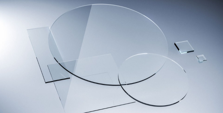
Applications of Glass Substrate
Role and Functions in Semiconductor Manufacturing
Glass substrates are essential in the semiconductor manufacturing process due to their unique material properties. They provide a stable and inert platform, which is crucial for the precision and reliability required in semiconductor fabrication. Glass substrates offer excellent thermal stability, which helps in maintaining the integrity of semiconductor devices during high-temperature processing. Their superior electrical insulation properties prevent unwanted electrical interference, ensuring the proper functioning of electronic circuits. Additionally, glass substrates exhibit remarkable dimensional stability, which is vital for the intricate photolithography processes used to create semiconductor patterns.
Applications in Advanced Packaging Technologies
In advanced packaging technologies, glass substrates are used to enhance the performance and miniaturization of electronic devices. Here are some specific applications:
- Smartphones: Glass substrates are integral to the development of high-density interconnects in smartphones. They enable the creation of compact and efficient circuitry that supports faster processing speeds and greater functionality within the limited space of modern smartphones.
- Wearable Devices: The flexibility and durability of glass substrates make them ideal for wearable technology, where space is at a premium and durability is a necessity.
- Displays: In display technology, such as OLED and LCD screens, glass substrates provide a smooth and stable surface that enhances image quality and display longevity.
- High-Frequency Components: Glass substrates are also used in the packaging of high-frequency components, where their low dielectric constant and high resistance to electromagnetic interference are crucial.
- Optoelectronics: In optoelectronic devices, including sensors and photonic devices, glass substrates help in achieving the desired optical clarity and performance characteristics.
Emerging Technologies: As technology advances, the applications of glass substrates continue to expand. They are increasingly being explored for use in 3D packaging and system-in-package (SiP) solutions, where multiple semiconductor devices are integrated into a single package to reduce size and improve performance. The ongoing development of 5G and IoT devices also leverages the unique properties of glass substrates to meet the demands of higher data rates and more complex connectivity requirements.
Through these varied applications, glass substrates demonstrate their critical role in pushing the boundaries of what is possible in semiconductor technology and advanced electronic packaging.
Glass Substrate Manufacturers
Overview of Major Glass Substrate Manufacturers
Several leading companies specialize in the production of glass substrates, each offering unique products tailored to different applications in the semiconductor industry. Prominent manufacturers include Corning Incorporated, AGC Inc., Schott AG, and NEG (Nippon Electric Glass).
- Corning Incorporated: Known for its innovation in glass and ceramics, Corning produces glass substrates with exceptional purity and uniformity. Their Gorilla Glass, widely used in smartphones and tablets, is renowned for its toughness and scratch resistance, making it suitable for advanced packaging and consumer electronics.
- AGC Inc.: A key player in the glass industry, AGC offers high-quality glass substrates characterized by excellent thermal and chemical stability. Their products are used in various applications, including displays and semiconductor manufacturing, due to their precise dimensional control and low impurity levels.
- Schott AG: Schott specializes in high-tech materials, offering glass substrates that are notable for their optical clarity and thermal resistance. Their products are commonly used in optoelectronics and high-frequency components, where superior performance and reliability are critical.
- NEG (Nippon Electric Glass): NEG provides advanced glass substrates with high thermal and mechanical stability, suitable for use in semiconductor and display technologies. Their focus on innovation has led to the development of substrates that support the latest advancements in electronics and photonics.
Technological Advantages of Different Manufacturers
- Corning Incorporated:
- Technological Advancements: Corning’s expertise in material science allows them to produce glass substrates with unmatched toughness and scratch resistance. Their ion-exchange process enhances the durability of the glass, making it ideal for portable electronic devices.
- Product Features: Corning’s substrates are known for their thinness and lightweight properties, which are crucial for modern, slim electronic designs.
- AGC Inc.:
- Technological Advancements: AGC utilizes advanced manufacturing techniques to produce glass substrates with high dimensional accuracy and low defect rates. Their float glass process ensures uniform thickness and surface smoothness, essential for semiconductor applications.
- Product Features: AGC’s substrates offer superior thermal and chemical resistance, making them suitable for harsh manufacturing environments and high-temperature processes.
- Schott AG:
- Technological Advancements: Schott’s glass substrates are distinguished by their high optical quality and thermal stability. Their use of precision glass molding and coating technologies ensures substrates that meet the stringent requirements of optoelectronics and photonics.
- Product Features: Schott’s products provide excellent transmission properties and minimal optical distortion, which are critical for high-performance optical applications.
- NEG (Nippon Electric Glass):
- Technological Advancements: NEG leverages innovative glass composition and processing techniques to create substrates with high mechanical strength and thermal stability. Their continuous improvement in glass melting and forming processes results in substrates that meet the latest industry standards.
- Product Features: NEG’s substrates are known for their low coefficient of thermal expansion and high resistance to thermal shock, making them ideal for applications that involve rapid temperature changes.
Each of these manufacturers brings unique strengths and innovations to the production of glass substrates, contributing to advancements in semiconductor and electronic device manufacturing. By leveraging their technological expertise and specialized products, these companies support the ongoing evolution of the semiconductor industry, enabling more powerful, efficient, and durable electronic devices.
Industrial Applications of Glass Substrate
Analyzing Real-World Cases of Intel Utilizing Glass Substrate in Semiconductor Manufacturing
Intel, a global leader in semiconductor manufacturing, has been at the forefront of integrating glass substrates into its production processes. One notable example is Intel’s use of glass substrates in the development of its advanced 3D packaging technology, known as Foveros. Foveros technology allows for the vertical stacking of chips, enabling higher performance and power efficiency in a smaller footprint. Glass substrates play a crucial role in this technology by providing a stable and thermally conductive platform for chip assembly.
Case Study: Intel’s Foveros Technology
- Role of Glass Substrate: In the Foveros packaging process, glass substrates are used as interposers, which are intermediate layers that facilitate communication between different chiplets stacked vertically. The high precision and excellent thermal properties of glass substrates help in maintaining the integrity of the stacked chips and ensure efficient heat dissipation.
- Advantages: The use of glass substrates in Foveros technology offers several benefits, including improved signal integrity, reduced power consumption, and enhanced thermal management. These advantages contribute to the overall performance and reliability of Intel’s processors, enabling more powerful and compact computing solutions.
Discussing the Cases and Advantages of TSMC Using Glass Substrate in Advanced Packaging Technologies
TSMC (Taiwan Semiconductor Manufacturing Company) is another major player in the semiconductor industry that has embraced the use of glass substrates in its advanced packaging solutions. TSMC’s innovations in chip packaging, particularly its Integrated Fan-Out (InFO) and Chip-on-Wafer-on-Substrate (CoWoS) technologies, have benefited significantly from the integration of glass substrates.
Case Study: TSMC’s InFO and CoWoS Technologies
- InFO Technology: TSMC’s InFO technology utilizes glass substrates to create ultra-thin packages with high interconnect density. Glass substrates offer superior planarity and dimensional stability, which are essential for achieving the fine-pitch interconnections required in modern semiconductor devices. This technology is widely used in high-performance applications, such as in the latest smartphones and tablets.
- Advantages: The use of glass substrates in InFO packaging results in thinner and lighter devices with enhanced electrical performance and thermal management. This contributes to the overall efficiency and longevity of consumer electronics.
- CoWoS Technology: In TSMC’s CoWoS technology, glass substrates serve as a robust and reliable platform for integrating multiple chips into a single package. This technology is particularly useful in high-performance computing and artificial intelligence applications, where large amounts of data need to be processed rapidly.
- Advantages: Glass substrates in CoWoS packaging offer excellent thermal conductivity and low dielectric loss, which are crucial for maintaining the performance and reliability of high-speed computing systems. The use of glass also allows for better scalability and integration of more complex designs.
C
The use of glass substrates by industry giants like Intel and TSMC highlights their critical role in advancing semiconductor manufacturing and packaging technologies. Intel’s Foveros technology and TSMC’s InFO and CoWoS solutions demonstrate the numerous advantages of glass substrates, including improved thermal management, enhanced electrical performance, and the ability to support more complex and compact designs. These real-world applications underscore the importance of glass substrates in driving innovation and enabling the development of next-generation electronic devices.
Technical Specifications and Pricing of Glass Substrate
Analysis of Glass Substrate Packaging Technologies and Forms
Glass substrates are employed in various packaging technologies due to their unique properties, such as high thermal stability, electrical insulation, and dimensional accuracy. Here, we delve into the different packaging technologies and forms that utilize glass substrates:
- Chip-on-Glass (COG):
- Technology: COG technology involves directly mounting semiconductor chips onto a glass substrate. This method is widely used in LCD displays and other flat panel displays where the glass substrate provides a stable and transparent base for the display components.
- Advantages: COG packaging benefits from the excellent optical properties of glass, which ensures high-quality display performance. The glass substrate’s stability and smooth surface help in achieving precise alignment and bonding of the chips.
- Glass Interposers:
- Technology: Glass interposers are used as intermediate layers in 2.5D and 3D packaging, connecting multiple chips within a single package. The glass interposer facilitates electrical connections through fine-pitch Through-Glass Vias (TGVs) and Redistribution Layers (RDLs).
- Advantages: Glass interposers offer superior thermal and electrical properties compared to traditional silicon interposers. They provide lower signal loss, better thermal management, and higher mechanical stability, making them ideal for high-performance computing and advanced data centers.
- Integrated Fan-Out (InFO):
- Technology: InFO technology by TSMC incorporates glass substrates to create ultra-thin, high-density packages. Glass substrates provide the necessary planarity and stability for fine-pitch interconnections and multilayer routing.
- Advantages: The use of glass substrates in InFO packaging results in thinner, lighter, and more efficient electronic devices. The superior electrical performance and thermal properties of glass substrates enhance the overall functionality and reliability of the packaged chips.
- System-in-Package (SiP):
- Technology: SiP technology integrates multiple semiconductor components into a single package. Glass substrates serve as the foundational layer, providing structural support and facilitating electrical connections between different components.
- Advantages: Glass substrates in SiP packaging offer excellent mechanical stability and thermal management, ensuring the reliable operation of complex, multifunctional electronic systems.
Exploring Pricing Factors and Market Trends of Glass Substrate
The pricing of glass substrates is influenced by several factors, including material properties, manufacturing processes, and market demand. Key factors affecting the pricing and market trends are as follows:
- Material Properties:
- Quality and Purity: Higher purity and quality glass substrates, which have fewer defects and impurities, command a premium price. These substrates are essential for high-performance applications where precision and reliability are critical.
- Thickness and Size: The thickness and size of the glass substrate also impact its cost. Thinner substrates and larger sizes often require more advanced manufacturing techniques, increasing production costs.
- Manufacturing Processes:
- Advanced Techniques: The use of advanced manufacturing processes such as precision glass molding, ion-exchange strengthening, and chemical vapor deposition (CVD) contributes to higher production costs. These techniques are necessary to achieve the desired properties and performance characteristics of the glass substrate.
- Yield Rates: The efficiency and yield rates of the manufacturing process significantly influence pricing. Higher yield rates lead to lower production costs per unit, while lower yields increase the cost.
- Market Demand:
- Industry Trends: The growing demand for advanced electronic devices, such as smartphones, wearables, and high-performance computing systems, drives the demand for high-quality glass substrates. This increased demand can lead to higher prices, especially for substrates with specialized properties.
- Supply Chain Dynamics: The availability of raw materials, manufacturing capacity, and competition among suppliers also impact the pricing of glass substrates. Disruptions in the supply chain or increased competition can lead to price fluctuations.
Market Trends:
- Technological Advancements: As semiconductor and electronic device technologies continue to advance, the demand for glass substrates with higher performance characteristics is expected to grow. Innovations in packaging technologies, such as 3D integration and heterogeneous integration, will drive the need for more sophisticated glass substrates.
- Cost Reduction Efforts: Manufacturers are continually working to improve production efficiency and reduce costs. Advancements in manufacturing techniques and increased automation are expected to lower the cost of glass substrates over time.
- Sustainability Initiatives: The semiconductor industry is increasingly focusing on sustainability. Manufacturers are exploring eco-friendly materials and processes to reduce the environmental impact of glass substrate production, which may also influence pricing and market trends.
The technical specifications and pricing of glass substrates are shaped by a combination of material properties, manufacturing processes, and market demand. Glass substrates play a crucial role in various advanced packaging technologies, offering superior performance and reliability. As the semiconductor industry evolves, the demand for high-quality glass substrates is expected to grow, driving further innovations and developments in this critical component of electronic manufacturing.
Advantages of Glass Substrate
Comparative Analysis of the Pros and Cons of Glass Substrate Against Other Common Substrate Materials
When evaluating glass substrates, it’s important to compare them against other common substrate materials like silicon, ceramic, and organic substrates. Each material has its own set of characteristics that make it suitable for specific applications.
Glass vs. Silicon
- Pros of Glass:
- Thermal Stability: Glass substrates have excellent thermal stability, which makes them suitable for high-temperature processing without warping or degradation.
- Electrical Insulation: Glass is an outstanding electrical insulator, reducing the risk of electrical interference and signal crosstalk in electronic circuits.
- Dimensional Stability: Glass maintains its shape and size under various conditions, ensuring precision in semiconductor manufacturing.
- Cons of Glass:
- Mechanical Fragility: Glass is more fragile than silicon, making it more susceptible to cracking and breaking under mechanical stress.
- Manufacturing Complexity: Processing glass can be more complex and expensive compared to silicon, particularly for cutting and handling.
Glass vs. Ceramic
- Pros of Glass:
- Optical Clarity: Unlike ceramic substrates, glass offers superior optical clarity, which is beneficial in optoelectronic applications.
- Surface Smoothness: Glass provides a smoother surface, essential for high-precision photolithography.
- Cons of Glass:
- Thermal Conductivity: Ceramics typically have better thermal conductivity than glass, making ceramics more suitable for applications requiring efficient heat dissipation.
- Cost: Ceramic substrates can sometimes be less expensive than high-quality glass substrates, depending on the application and specifications.
Glass vs. Organic Substrates
- Pros of Glass:
- Environmental Stability: Glass substrates are more resistant to environmental factors such as moisture, temperature fluctuations, and chemical exposure compared to organic substrates.
- Long-Term Reliability: Glass does not degrade over time like organic materials, ensuring longer-lasting performance in electronic devices.
- Cons of Glass:
- Flexibility: Organic substrates are more flexible, making them suitable for applications where bending and flexing are required, such as flexible electronics.
- Cost and Weight: Organic substrates are generally lighter and cheaper to produce than glass substrates.
Discussing the Technical Advantages and Development Potential of Glass Substrate in Semiconductor Manufacturing
Technical Advantages
- Superior Electrical Properties:
- Insulation: The high dielectric strength of glass makes it an excellent insulator, reducing the risk of electrical shorts and improving overall device reliability.
- Low Dielectric Constant: Glass substrates have a low dielectric constant, which minimizes signal loss and enhances the performance of high-frequency circuits.
- Thermal Management:
- Thermal Stability: Glass substrates can withstand high processing temperatures, making them ideal for applications involving high thermal loads.
- Heat Dissipation: While glass itself is not highly thermally conductive, its stability allows for the integration of additional thermal management solutions, such as thermal vias or metal layers.
- Precision and Stability:
- Dimensional Accuracy: The high dimensional stability of glass ensures precise alignment and patterning, which is crucial for advanced semiconductor manufacturing techniques like photolithography.
- Surface Quality: The smooth and defect-free surface of glass substrates supports high-resolution patterning and reduces the likelihood of defects in semiconductor devices.
- Optical Properties:
- Transparency: Glass substrates are highly transparent, which is essential for applications in optoelectronics, including displays, sensors, and photovoltaic cells.
- Optical Clarity: The optical clarity of glass substrates ensures minimal distortion and high performance in devices requiring precise light manipulation.
Development Potential
- Advanced Packaging Technologies:
- Glass substrates are increasingly used in advanced packaging technologies such as 2.5D and 3D integration, where their superior properties enable the stacking and interconnection of multiple chips. This contributes to the development of more powerful and compact electronic devices.
- 5G and IoT Applications:
- The rise of 5G and Internet of Things (IoT) technologies demands substrates that can handle high frequencies and dense interconnections. Glass substrates, with their excellent electrical and thermal properties, are well-suited to meet these requirements, driving innovation in communication and connectivity solutions.
- Flexible and Wearable Electronics:
- While traditionally considered rigid, advancements in glass processing techniques are leading to the development of flexible glass substrates. These innovations open new possibilities for their use in flexible and wearable electronics, combining the robustness of glass with the flexibility needed for new form factors.
- Sustainability and Cost Reduction:
- As the semiconductor industry moves towards more sustainable practices, glass substrates offer an environmentally friendly alternative to some traditional materials. Ongoing research and development aim to reduce the cost of producing high-quality glass substrates, making them more accessible for a wider range of applications.
C
Glass substrates offer a compelling combination of electrical insulation, thermal stability, dimensional accuracy, and optical clarity, making them highly advantageous for semiconductor manufacturing and advanced packaging technologies. Despite some challenges, such as mechanical fragility and manufacturing complexity, the continued development and innovation in glass substrate technology promise to enhance their role in the future of electronics. The unique properties and growing applications of glass substrates underscore their potential to drive significant advancements in semiconductor technology and electronic device manufacturing.
Glass Core Substrate
Explanation of the Concept and Characteristics of Glass Core Substrate
Glass core substrate refers to a specialized type of substrate where the core material is made primarily of glass. Unlike traditional substrates that may have a different core material, such as silicon or ceramic, glass core substrates leverage the unique properties of glass as the primary structural component.
Characteristics of Glass Core Substrate
- Thermal Stability: Glass core substrates exhibit excellent thermal stability, allowing them to withstand high processing temperatures encountered during semiconductor manufacturing without warping or deformation.
- Electrical Insulation: Glass is an exceptional electrical insulator, minimizing the risk of electrical interference and ensuring the integrity of electronic circuits.
- Dimensional Accuracy: Glass core substrates offer high dimensional accuracy, providing a stable and precise platform for semiconductor device fabrication. This characteristic is crucial for maintaining alignment and patterning accuracy in advanced semiconductor processes.
- Surface Smoothness: The smooth surface of glass core substrates supports high-resolution patterning and reduces the risk of defects in semiconductor devices. It enables precise photolithography processes necessary for creating intricate semiconductor patterns.
- Optical Clarity: Glass core substrates are highly transparent, making them suitable for optoelectronic applications where optical clarity is essential. They allow for efficient light transmission and manipulation in devices such as displays, sensors, and photovoltaic cells.
Exploration of the Application Prospects of Glass Core Substrate in Semiconductor Manufacturing
- Advanced Packaging Technologies:
- Glass core substrates have significant potential in advanced packaging technologies, particularly in 3D integration and system-in-package (SiP) solutions. Their thermal stability, electrical insulation, and dimensional accuracy make them well-suited for integrating multiple semiconductor components into compact and efficient packages.
- Optoelectronic Devices:
- Glass core substrates are ideal for optoelectronic devices that require precise light manipulation and transmission. They can be used as substrates for photonic integrated circuits (PICs), optical sensors, and light-emitting diodes (LEDs), where optical clarity and stability are paramount.
- High-Frequency Components:
- In high-frequency applications such as RF/microwave devices and millimeter-wave systems, glass core substrates offer low dielectric loss and excellent signal integrity. They can support the development of high-performance components for wireless communication, radar systems, and automotive applications.
- Miniaturization and Wearable Electronics:
- Glass core substrates enable the miniaturization of electronic devices and support the development of wearable electronics. Their lightweight and durable properties make them suitable for applications where size, weight, and reliability are critical, such as smartwatches, fitness trackers, and medical devices.
- Emerging Technologies:
- As semiconductor technology continues to advance, glass core substrates are expected to find new applications in emerging technologies such as quantum computing, neuromorphic computing, and advanced sensing systems. Their unique combination of properties makes them versatile substrates for supporting cutting-edge innovations in the semiconductor industry.
Glass core substrates offer a compelling combination of thermal stability, electrical insulation, dimensional accuracy, and optical clarity, making them well-suited for a wide range of semiconductor manufacturing applications. Their potential in advanced packaging technologies, optoelectronic devices, high-frequency components, miniaturization, and emerging technologies underscores their importance in driving innovation and advancement in the semiconductor industry. As research and development efforts continue to enhance their properties and manufacturing processes, glass core substrates are poised to play a significant role in shaping the future of electronic devices and semiconductor technology.
Feasibility of Glass as a Substrate
Glass has gained considerable attention as a potential semiconductor substrate due to its unique properties and versatile applications. Here, we delve into the feasibility of using glass as a substrate in semiconductor manufacturing, analyzing its advantages and limitations across different application scenarios.
Advantages of Glass as a Semiconductor Substrate
- Thermal Stability: Glass exhibits excellent thermal stability, allowing it to withstand high processing temperatures encountered during semiconductor fabrication without warping or deformation. This property ensures the integrity and reliability of semiconductor devices, particularly in high-temperature processes like deposition and annealing.
- Electrical Insulation: Glass is an outstanding electrical insulator, reducing the risk of electrical interference and ensuring the proper functioning of electronic circuits. Its low dielectric constant and high resistivity make it suitable for applications requiring precise control of electrical properties, such as RF/microwave devices and high-frequency components.
- Dimensional Accuracy: Glass substrates offer high dimensional accuracy, providing a stable and precise platform for semiconductor device fabrication. This characteristic is crucial for maintaining alignment and patterning accuracy in advanced semiconductor processes like photolithography and etching.
- Optical Clarity: Glass substrates are highly transparent, making them ideal for optoelectronic applications where optical clarity is essential. They allow for efficient light transmission and manipulation in devices such as displays, sensors, and photovoltaic cells, enabling high-performance optoelectronic systems.
- Environmental Stability: Glass is resistant to environmental factors such as moisture, temperature fluctuations, and chemical exposure, ensuring long-term reliability and stability in semiconductor devices. This property makes glass substrates suitable for harsh operating conditions and outdoor applications, where reliability is paramount.
Limitations of Glass as a Semiconductor Substrate
- Mechanical Fragility: Glass is more fragile than traditional semiconductor substrates like silicon and ceramic, making it susceptible to cracking and breaking under mechanical stress. This limitation poses challenges in handling and processing glass substrates, particularly in applications requiring high mechanical strength and durability.
- Cost: The cost of manufacturing glass substrates can be higher compared to other substrate materials, particularly for high-purity and high-quality glass. Processing glass requires specialized equipment and techniques, contributing to higher production costs and potentially limiting its adoption in cost-sensitive applications.
- Thermal Conductivity: While glass offers excellent thermal stability, its thermal conductivity is lower compared to materials like silicon and ceramic. This limitation may impact heat dissipation in semiconductor devices, particularly in high-power applications where efficient thermal management is critical.
- Flexibility: Glass substrates are inherently rigid, limiting their suitability for applications requiring flexible or bendable electronics. Unlike organic substrates, which offer flexibility and conformability, glass substrates are not well-suited for applications where mechanical flexibility is essential.
The feasibility of using glass as a semiconductor substrate depends on various factors, including application requirements, performance criteria, and cost considerations. While glass offers several advantages such as thermal stability, electrical insulation, and dimensional accuracy, its limitations in terms of mechanical fragility, cost, thermal conductivity, and flexibility need to be carefully evaluated. Despite these challenges, ongoing research and development efforts aim to address these limitations and expand the use of glass substrates in semiconductor manufacturing, particularly in applications where their unique properties offer distinct advantages. As technology continues to evolve, glass substrates are expected to play an increasingly important role in enabling next-generation semiconductor devices and electronic systems.
Raw Materials for Glass Substrate
Glass substrates are manufactured using a combination of raw materials and specialized processes to achieve the desired properties and performance characteristics. Here, we explore the manufacturing materials and processes involved in producing glass substrates for semiconductor applications.
Raw Materials
a. Silica (Silicon Dioxide): Silica is the primary component of glass substrates, typically sourced from sand, quartz, or other silica-rich minerals. It serves as the main network former, providing structural integrity and stability to the glass matrix.
b. Fluxes: Fluxes such as soda ash (sodium carbonate) and limestone (calcium carbonate) are added to lower the melting point of silica and improve glass meltability. These fluxes facilitate the formation of a homogeneous glass melt and help in reducing the viscosity of the molten glass.
c. Stabilizers: Stabilizers like alumina (aluminum oxide) or boron oxide are often added to enhance the chemical durability and thermal shock resistance of glass substrates. These additives help in controlling the expansion coefficient and preventing glass degradation under harsh conditions.
d. Colorants and Additives: Depending on the application and desired properties, colorants such as metal oxides (e.g., iron oxide, cobalt oxide) may be added to impart specific colors or optical characteristics to the glass substrate. Other additives like rare earth elements or dopants may also be included to modify the electrical or optical properties of the glass.
Manufacturing Processes
a. Melting: The raw materials are batched and mixed according to the desired composition, then melted in a high-temperature furnace (typically at temperatures exceeding 1500°C). The melting process converts the raw materials into a homogenous liquid glass melt.
b. Forming: The molten glass is then formed into a flat sheet or slab using various techniques such as float glass process, draw-down process, or fusion draw process. In the float glass process, the molten glass is poured onto a bath of molten tin, where it spreads out and forms a continuous ribbon of glass with uniform thickness.
c. Annealing: After forming, the glass substrate undergoes annealing to relieve internal stresses and improve its mechanical strength and dimensional stability. The glass is slowly cooled in a controlled manner to prevent cracking or warping.
d. Cutting and Polishing: The glass substrate is cut into the desired size and shape using precision cutting tools. The edges are then polished to remove any sharp edges or surface imperfections, ensuring a smooth and uniform finish.
e. Surface Treatment: Depending on the application, the surface of the glass substrate may undergo various treatments such as chemical etching, coating deposition, or surface modification to enhance its properties or functionality.
f. Quality Control: Throughout the manufacturing process, stringent quality control measures are implemented to ensure the final glass substrates meet the required specifications and performance standards. This includes testing for dimensional accuracy, optical clarity, surface smoothness, and chemical durability.
The manufacturing of glass substrates involves a complex interplay of raw materials and processes to produce high-quality substrates with tailored properties for semiconductor applications. By carefully selecting the raw materials and optimizing the manufacturing processes, glass substrate manufacturers can achieve precise control over the composition, structure, and performance of the final product. As semiconductor technology continues to advance, ongoing research and development efforts in glass substrate manufacturing aim to further enhance the properties and capabilities of glass substrates, enabling new opportunities for innovation and advancement in the semiconductor industry.
FAQs About what is glass substrate
A glass core substrate refers to a specialized type of substrate used in various industries, including electronics and optics. Unlike traditional substrates made from materials like silicon or ceramic, a glass core substrate primarily consists of glass material. It serves as a foundational layer for building electronic or optical components, providing structural support, electrical insulation, and thermal stability. Glass core substrates are commonly utilized in applications where high precision, dimensional accuracy, and optical clarity are essential, such as semiconductor manufacturing, optoelectronics, and photonics.
Yes, glass can be used as a substrate in various applications across different industries. Glass substrates offer several advantages, including thermal stability, electrical insulation, optical clarity, and dimensional accuracy, making them suitable for a wide range of applications. In the semiconductor industry, glass substrates are used as interposers, carriers, or base materials for fabricating electronic devices and integrated circuits. They are also utilized in optoelectronic devices, displays, sensors, and photovoltaic cells, where optical transparency and stability are critical.
The raw materials used for manufacturing glass substrates typically include:
Silica (Silicon Dioxide): The primary component of glass, sourced from sand, quartz, or other silica-rich minerals.
Fluxes: Additives such as soda ash (sodium carbonate) and limestone (calcium carbonate) to lower the melting point of silica and improve glass meltability.
Stabilizers: Materials like alumina (aluminum oxide) or boron oxide to enhance the chemical durability and thermal shock resistance of glass substrates.
Colorants and Additives: Metal oxides (e.g., iron oxide, cobalt oxide) for imparting specific colors or optical characteristics to the glass, as well as rare earth elements or dopants for modifying its electrical or optical properties.
The advantages of glass substrate include:
Thermal Stability: Glass substrates offer excellent thermal stability, allowing them to withstand high processing temperatures without warping or deformation.
Electrical Insulation: Glass is an outstanding electrical insulator, reducing the risk of electrical interference and ensuring the integrity of electronic circuits.
Optical Clarity: Glass substrates are highly transparent, making them suitable for applications where optical clarity is essential, such as displays and sensors.
Dimensional Accuracy: Glass substrates provide high dimensional accuracy, ensuring precise alignment and patterning in semiconductor manufacturing processes.
Environmental Stability: Glass substrates are resistant to environmental factors such as moisture, temperature fluctuations, and chemical exposure, ensuring long-term reliability and stability in electronic devices.

