
Optimizing Substrate Layout for PCB Performance
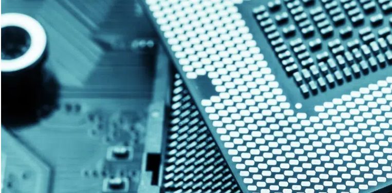
Printed Circuit Boards (PCBs) are the backbone of modern electronic devices, serving as the platform for mounting and interconnecting various electronic components. They are crucial in ensuring the functionality and reliability of everything from simple gadgets to complex machinery. PCBs provide mechanical support and establish electrical connections through conductive pathways etched from copper sheets laminated onto a non-conductive substrate. This structured layout allows for the compact and efficient design of electronic circuits, enabling the development of smaller, faster, and more powerful devices.
The purpose of this article is to delve into the concept of substrate layout within PCB design. Understanding substrate layout is essential for optimizing PCB performance, ensuring signal integrity, and enhancing overall device reliability. By exploring different types of substrates, materials used, and the significance of dielectric properties, this article aims to provide a comprehensive overview of how substrate layout influences PCB design and functionality.
What is a Substrate in a PCB?
The substrate in a Printed Circuit Board (PCB) is the foundational material upon which the entire board is constructed. It serves several critical roles in the overall structure and functionality of the PCB. Primarily, the substrate provides mechanical support, giving the PCB its rigidity and shape. This is essential for maintaining the integrity of the board, ensuring that it can withstand physical stress and environmental factors during both assembly and operation.
Functionally, the substrate acts as an insulating layer between the conductive layers of the PCB. It ensures that electrical signals are properly directed through the intended pathways without unintended interference. The substrate’s dielectric properties are crucial for maintaining signal integrity, particularly in high-frequency applications where even small losses can significantly impact performance.
In terms of supporting and connecting other electronic components, the substrate is typically made from materials like FR4 (a fiberglass-reinforced epoxy laminate), which offers a balance of strength, durability, and electrical insulation. The substrate’s surface is coated with a thin layer of copper, which is then etched to create the intricate network of conductive traces that interconnect various electronic components, such as resistors, capacitors, and integrated circuits.
These components are soldered onto the substrate, and the copper traces allow for electrical signals to travel between them, enabling the desired circuit functions. Additionally, vias—small holes drilled through the substrate and filled with conductive material—allow for connections between different layers of the PCB, facilitating more complex and compact designs.
By providing both structural support and electrical insulation, the substrate plays a fundamental role in the reliable performance of PCBs, making it an indispensable element in the design and manufacture of electronic devices.
Types of PCB Substrates
In PCB design, the choice of substrate material is crucial as it directly impacts the board’s performance, durability, and application suitability. Here is an overview of some common types of PCB substrates:
FR4 (Fiberglass Epoxy Resin)
FR4 is the most widely used PCB substrate material due to its excellent balance of properties. It consists of woven fiberglass cloth with an epoxy resin binder, making it durable and flame-resistant. FR4 offers good mechanical strength, electrical insulation, and moderate cost, making it suitable for a wide range of applications, from consumer electronics to industrial equipment. Its high dielectric strength and low moisture absorption ensure reliability in various environmental conditions.
CEM-1 and CEM-3
Composite Epoxy Material (CEM) substrates are similar to FR4 but with different compositions and properties.
- CEM-1: Made of paper core laminated with epoxy resin and woven glass, CEM-1 is less expensive than FR4 but offers lower mechanical and electrical performance. It is typically used in single-layer PCBs for low-cost, low-performance applications.
- CEM-3: This material is made of woven glass fabric with a paper core, similar to CEM-1, but with improved performance. CEM-3 offers better mechanical strength and electrical properties compared to CEM-1, making it suitable for double-layer PCBs used in moderate-performance applications.
High-Frequency Materials (e.g., Rogers)
High-frequency substrates, such as those made by Rogers Corporation, are designed for applications requiring high-speed signal transmission and minimal signal loss. These materials typically have low dielectric constants and low loss tangents, which are essential for maintaining signal integrity at high frequencies. Rogers materials, such as RO4350B and RO4003C, are commonly used in RF (radio frequency) and microwave PCBs, where performance and precision are critical. These substrates are often used in telecommunications, aerospace, and advanced computing applications.
Metal Substrates (e.g., Aluminum Substrates)
Metal substrates, especially aluminum-based ones, are used in applications requiring excellent heat dissipation and mechanical strength. These substrates consist of a metal base layer (usually aluminum), a dielectric layer, and a copper circuit layer. Aluminum substrates are ideal for power electronics, LED lighting, and automotive applications, where efficient heat management is essential. The metal base helps to dissipate heat away from critical components, thereby enhancing the PCB’s thermal performance and reliability.
Each type of substrate material brings unique advantages and is chosen based on the specific requirements of the application. Understanding these materials’ properties and applications is crucial for optimizing PCB design and ensuring the final product’s performance and durability.
PCB Substrate Materials
Choosing the right substrate material for a PCB is vital for ensuring the board’s performance, reliability, and suitability for specific applications. Different types of substrates use various materials, each offering distinct characteristics that cater to diverse requirements. Here’s a detailed look at the materials used for different types of substrates and their key attributes and applications:
FR4 (Fiberglass Epoxy Resin)
FR4 is composed of a woven fiberglass cloth impregnated with epoxy resin. This combination provides a robust and versatile material widely used in PCB manufacturing.
- Characteristics:
- Heat Resistance: FR4 can withstand high temperatures without degrading, making it suitable for a wide range of thermal environments.
- Mechanical Strength: The fiberglass reinforcement provides excellent mechanical strength and durability.
- Electrical Insulation: The epoxy resin offers good electrical insulation, ensuring signal integrity and preventing short circuits.
- Cost-Effectiveness: FR4 is relatively inexpensive compared to other high-performance materials, making it a cost-effective choice for many applications.
- Applications:
- Consumer electronics (e.g., smartphones, computers)
- Industrial equipment
- Automotive electronics
- General-purpose PCBs
CEM-1 and CEM-3
Composite Epoxy Materials (CEM) are alternatives to FR4, with slightly different compositions and properties.
- CEM-1:
- Materials: Made from a paper core with a single layer of woven glass and epoxy resin.
- Characteristics: Lower mechanical and electrical performance compared to FR4, but still provides adequate insulation and support for simpler circuits.
- Applications: Single-layer PCBs used in low-cost, low-performance devices, such as simple consumer electronics and household appliances.
- CEM-3:
- Materials: Consists of a woven glass fabric core with a paper layer, impregnated with epoxy resin.
- Characteristics: Better mechanical strength and electrical properties than CEM-1, but slightly less than FR4.
- Applications: Double-layer PCBs for moderate-performance applications, such as office equipment and certain consumer electronics.
High-Frequency Materials (e.g., Rogers)
High-frequency substrates are designed for applications requiring minimal signal loss and high-speed signal transmission.
- Materials: Typically use materials like PTFE (Teflon), ceramic-filled composites, or other advanced polymers.
- Characteristics:
- Low Dielectric Loss: Essential for maintaining signal integrity at high frequencies.
- High-Frequency Performance: Superior performance in RF and microwave applications due to low dielectric constant and loss tangent.
- Thermal Stability: Maintains consistent electrical properties over a wide temperature range.
- Applications:
- Telecommunications (e.g., antennas, RF modules)
- Aerospace and defense systems
- High-speed computing
- Advanced medical equipment
Metal Substrates (e.g., Aluminum Substrates)
Metal substrates incorporate a metal base layer, usually aluminum, to enhance thermal management and mechanical support.
- Materials: Consist of an aluminum base, a dielectric layer, and a copper circuit layer.
- Characteristics:
- Excellent Heat Dissipation: The metal base efficiently dissipates heat away from critical components, preventing overheating and extending component life.
- Mechanical Strength: Provides robust mechanical support, especially in high-stress environments.
- Thermal Conductivity: High thermal conductivity of the metal base ensures effective heat management.
- Applications:
- Power electronics (e.g., power supplies, motor controllers)
- LED lighting systems
- Automotive electronics (e.g., engine control units, lighting systems)
- Industrial power modules
Each type of PCB substrate material offers unique advantages tailored to specific applications. By understanding these materials’ properties and applications, designers can make informed decisions to optimize PCB performance and ensure the final product’s reliability and efficiency.
Substrate Layout in PCB Design
The substrate layout is a crucial aspect of PCB design, as it directly affects the board’s performance, signal integrity, and overall reliability. A well-planned substrate layout ensures that the electronic components function correctly and efficiently, minimizing issues like signal interference, power distribution problems, and thermal management challenges.
The Importance of Substrate Layout in PCB Design
The substrate layout is vital for several reasons:
- Signal Integrity: Properly designing the substrate layout helps maintain signal integrity by minimizing noise, crosstalk, and electromagnetic interference (EMI). This is particularly important in high-speed and high-frequency applications where even minor disruptions can lead to significant performance degradation.
- Power Distribution: Efficient power distribution is essential for the reliable operation of electronic components. A well-designed substrate layout ensures that power is delivered uniformly across the PCB, preventing voltage drops and ensuring stable operation.
- Thermal Management: Effective thermal management is crucial to prevent overheating and extend the lifespan of electronic components. The substrate layout, including the placement of thermal vias and heat sinks, plays a significant role in dissipating heat away from critical components.
- Mechanical Stability: The substrate layout contributes to the mechanical stability of the PCB, ensuring that it can withstand physical stresses during manufacturing, assembly, and operation. This includes considerations for board thickness, material selection, and the arrangement of layers.
Functions of Different Layers
In a multi-layer PCB, various layers are designed to serve specific functions, ensuring optimal performance and reliability. The key layers include:
- Signal Layer
- Function: The signal layer is dedicated to routing electrical signals between different components on the PCB. It carries data, control, and clock signals essential for the functioning of the circuit.
- Design Considerations: Signal layers should be designed to minimize signal interference and crosstalk. This involves careful trace routing, maintaining consistent trace width, and using appropriate spacing between traces. High-speed signals may require controlled impedance routing and differential pair routing.
- Power Layer
- Function: The power layer is responsible for distributing power to various components on the PCB. It ensures that each component receives the correct voltage and current required for operation.
- Design Considerations: Power layers should be designed with sufficient copper thickness to handle the required current without excessive voltage drops. Decoupling capacitors should be strategically placed to filter out noise and stabilize the power supply. Power planes can also help distribute heat and reduce EMI.
- Ground Layer
- Function: The ground layer provides a common return path for electrical currents and serves as a reference point for all signals on the PCB. It helps in reducing noise and improving signal integrity by providing a low-impedance path for return currents.
- Design Considerations: A solid ground plane is essential for reducing EMI and ensuring stable operation. It should cover as much area as possible to provide effective grounding. Ground planes also play a crucial role in thermal management, helping to dissipate heat from components.
By carefully designing the substrate layout and understanding the functions of different layers, engineers can optimize PCB performance and reliability. This involves not only selecting the appropriate substrate materials but also strategically planning the placement of components, traces, and vias to achieve the desired electrical and thermal characteristics.
Dielectric Substrate
Introduction to Dielectric Substrates and Their Application in High-Frequency and High-Performance PCBs
Dielectric substrates are materials used in PCB design that possess insulating properties, essential for separating conductive layers and ensuring proper signal propagation. These substrates play a critical role in high-frequency and high-performance PCBs, where maintaining signal integrity and minimizing losses are paramount. Dielectric substrates are chosen based on their electrical properties, particularly the dielectric constant and loss factor, which directly influence the performance of high-speed and RF (radio frequency) circuits.
In high-frequency and high-performance applications, dielectric substrates must support the rapid transmission of signals without significant attenuation or distortion. Materials like PTFE (Teflon), ceramic-filled composites, and other advanced polymers are commonly used due to their favorable electrical characteristics. These substrates are essential in applications such as telecommunications, aerospace, advanced computing, and medical devices, where precision and reliability are critical.
Impact of Dielectric Constant and Loss Factor
The dielectric constant (Dk) and loss factor (Df) are two fundamental properties that impact the performance of dielectric substrates in PCBs.
Dielectric Constant (Dk)
The dielectric constant, also known as the relative permittivity, measures a material’s ability to store electrical energy in an electric field. It is a crucial parameter in determining the speed at which signals travel through the substrate. A lower dielectric constant typically results in faster signal propagation and reduced signal delay, which is vital for high-frequency applications.
- Impact on Signal Speed: A lower Dk allows for higher signal speeds, essential for high-frequency circuits. Materials with low dielectric constants are preferred in RF and microwave PCBs to ensure rapid signal transmission.
- Impedance Control: The dielectric constant affects the characteristic impedance of transmission lines. Precise control of Dk is necessary for maintaining consistent impedance, which is crucial for minimizing reflections and signal loss.
Loss Factor (Df)
The loss factor, or dissipation factor, indicates how much energy from the signal is lost as heat within the dielectric material. A lower loss factor means less signal attenuation and better performance, especially at high frequencies.
- Impact on Signal Integrity: A low Df is essential for maintaining signal integrity, as it minimizes signal loss and distortion. This is particularly important in high-frequency and high-speed applications where even small losses can degrade performance.
- Thermal Considerations: Materials with lower loss factors generate less heat, improving thermal management and reliability in high-performance PCBs.
Applications of Dielectric Substrates
Dielectric substrates are used in a variety of high-frequency and high-performance PCB applications:
- Telecommunications: In devices such as antennas, base stations, and RF modules, dielectric substrates with low Dk and Df are essential for ensuring clear and reliable signal transmission.
- Aerospace and Defense: High-performance PCBs in radar systems, satellite communications, and avionics require dielectric substrates that offer stable electrical properties under extreme conditions.
- Advanced Computing: High-speed data transmission in servers, data centers, and high-performance computing systems relies on dielectric substrates that support rapid signal propagation and minimal loss.
- Medical Devices: Precision and reliability in medical imaging equipment and diagnostic devices are achieved using high-performance dielectric substrates that ensure accurate signal processing.
In summary, dielectric substrates are a cornerstone of high-frequency and high-performance PCB design. By understanding and optimizing the dielectric constant and loss factor, engineers can significantly enhance the performance, reliability, and efficiency of electronic devices in demanding applications.
PCB Material Properties
Key Performance Parameters of PCB Materials
PCB materials exhibit a range of properties that directly influence their suitability for different applications. Understanding these key parameters helps in selecting the appropriate material for specific design requirements:
1. Dielectric Constant (Dk)
- Definition: The dielectric constant, or relative permittivity, measures a material’s ability to store electrical energy in an electric field relative to vacuum.
- Importance: Dk affects signal propagation speed and impedance control in PCBs.
- Low vs. High Dk: Lower Dk materials are preferred for high-frequency applications to minimize signal delay and loss. Higher Dk materials are used for impedance matching and controlled routing in certain designs.
- Applications: Critical in RF, microwave, and high-speed digital applications where signal integrity is paramount.
2. Coefficient of Thermal Expansion (CTE)
- Definition: CTE measures how much a material expands or contracts with changes in temperature.
- Importance: CTE affects PCB reliability by influencing mechanical stress, solder joint integrity, and dimensional stability.
- Low vs. High CTE: Materials with low CTE are preferred to minimize thermal stress during temperature cycling, ensuring long-term reliability.
- Applications: Crucial in electronics subjected to varying temperatures, such as automotive, aerospace, and industrial applications.
3. Thermal Conductivity
- Definition: Thermal conductivity measures a material’s ability to conduct heat.
- Importance: High thermal conductivity helps in dissipating heat generated by components, ensuring operational reliability and longevity.
- Materials: Metals like aluminum have high thermal conductivity, making them suitable for applications requiring efficient heat dissipation.
- Applications: Power electronics, LED lighting, and other high-power applications benefit from materials with high thermal conductivity to manage heat effectively.
4. Moisture Absorption
- Definition: Moisture absorption refers to the amount of moisture a material can absorb from the environment.
- Importance: Moisture absorption can degrade electrical properties, leading to increased signal loss and reduced insulation resistance.
- Low vs. High Absorption: Low moisture absorption materials are critical in humid environments or applications requiring long-term reliability.
- Materials: Epoxy resins used in PCB substrates typically have low moisture absorption rates, ensuring stable electrical performance over time.
- Applications: Consumer electronics, outdoor equipment, and applications exposed to varying humidity levels require materials with minimal moisture absorption.
Optimizing Material Selection
Selecting the right PCB material involves balancing these properties based on specific application requirements. For example, high-frequency PCBs prioritize low Dk and Df for signal integrity, while industrial PCBs focus on high thermal conductivity and low CTE for reliability under harsh conditions. By considering these key parameters, engineers can design PCBs that meet performance expectations and operational demands across diverse industries and applications.
Difference Between PCB and Package Substrate
Comparison of PCB Substrates and Package Substrates
PCB substrates and package substrates serve distinct roles in electronic packaging and circuit integration, each tailored to specific applications and design requirements.
PCB Substrates
- Definition: PCB substrates serve as the foundation for mounting and interconnecting electronic components, forming the basis of printed circuit boards.
- Applications: Used in a wide range of electronic devices and systems, including consumer electronics, telecommunications equipment, industrial controls, and automotive electronics.
- Characteristics:
- Complexity: PCBs can be single-layer, double-layer, or multi-layered structures, allowing for intricate circuit designs and high component density.
- Materials: Utilize materials like FR4, CEM-1, and high-frequency substrates depending on application requirements such as signal integrity, thermal management, and mechanical strength.
- Functionality: Designed to provide electrical interconnects, signal routing, power distribution, and mechanical support for various electronic components.
- Manufacturing: Produced through processes including etching, drilling, and soldering, involving intricate layout design and fabrication steps.
Package Substrates
- Definition: Package substrates are specialized materials used in the construction of semiconductor packages, such as integrated circuit (IC) packages and system-in-package (SiP) modules.
- Applications: Primarily used in semiconductor manufacturing and packaging industries, where ICs and other microelectronic devices require encapsulation and interconnection.
- Characteristics:
- Integration: Package substrates integrate multiple functions, including electrical interconnects, thermal management, and often include embedded passives (resistors, capacitors).
- Materials: Use materials optimized for thermal conductivity, low electrical parasitics, and mechanical reliability under varying conditions.
- Design: Tailored to specific IC designs, ensuring optimal performance, reliability, and miniaturization.
- Manufacturing: Involves advanced technologies such as flip-chip bonding, wire bonding, and encapsulation to ensure precise alignment and protection of ICs.
Comparison
- Functionality: PCB substrates focus on providing electrical connectivity and mechanical support for a broader range of electronic components and circuits. Package substrates, on the other hand, are specialized for encapsulating and interconnecting semiconductor devices with enhanced thermal and electrical performance.
- Applications: PCBs are versatile and used in diverse applications requiring reliable circuitry and interconnectivity. Package substrates are essential in semiconductor packaging, ensuring miniaturization, high performance, and reliability of ICs and SiPs.
- Materials: PCB substrates vary widely in material composition to meet different electrical, thermal, and mechanical requirements. Package substrates are typically engineered with materials optimized for specific semiconductor packaging needs, including thermal dissipation and electrical performance.
Understanding the differences between PCB substrates and package substrates is crucial for designing and manufacturing electronic systems and semiconductor devices effectively. Each type plays a critical role in enabling the functionality, reliability, and performance of modern electronic products across various industries and applications.
What is IC Substrate?
Explanation of IC Substrate and its Role in Integrated Circuit Packaging
An IC (Integrated Circuit) substrate serves as a foundational component in the packaging of semiconductor devices, providing mechanical support, electrical connectivity, and thermal management for integrated circuits. It plays a critical role in ensuring the functionality, reliability, and performance of ICs by facilitating the interconnection of semiconductor dies with external circuitry and components.
Materials and Design Considerations for IC Substrates
- Materials:
- Ceramic Substrates: Commonly used for high-performance IC packaging due to their excellent thermal conductivity, mechanical strength, and electrical insulation properties. Aluminum oxide (Al2O3) and aluminum nitride (AlN) are typical ceramic materials used.
- Organic Substrates: Utilized in cost-effective IC packaging solutions, organic substrates (e.g., BT resin) offer good electrical properties and are suitable for mainstream semiconductor packaging.
- Metallic Substrates: Aluminum and copper-based substrates are chosen for their superior thermal dissipation capabilities, crucial for high-power applications.
- Design Considerations:
- Electrical Connectivity: IC substrates must provide reliable electrical connections between the semiconductor die and external circuitry. This includes designing fine-pitch interconnects, vias, and bond pads to ensure low electrical resistance and signal integrity.
- Thermal Management: Effective heat dissipation is critical to prevent overheating and ensure the long-term reliability of ICs. IC substrate designs incorporate features like heat sinks, thermal vias, and metal layers to efficiently transfer heat away from the semiconductor die.
- Mechanical Support: IC substrates provide structural support to the semiconductor die and protect it from mechanical stresses during handling and operation. The substrate’s material and design must withstand thermal cycling and mechanical shock without compromising electrical performance.
- Advanced Packaging Technologies:
- Flip-Chip Bonding: Enables direct electrical connections between the IC die and substrate, reducing parasitic capacitance and improving signal integrity.
- Embedded Passives: Integrates passive components (resistors, capacitors) within the substrate layers, optimizing space utilization and enhancing circuit performance.
- Package-on-Package (PoP): Allows stacking of multiple IC substrates to increase functional density and performance in compact electronic devices.
Applications of IC Substrates
IC substrates are essential in various semiconductor packaging applications, including:
- Microprocessors and Microcontrollers: High-performance computing applications requiring efficient thermal management and electrical performance.
- Memory Devices: DRAM and NAND flash memory packages benefit from IC substrates that ensure reliable electrical connections and thermal dissipation.
- RF and Microwave Devices: IC substrates with low-loss materials are critical for high-frequency signal transmission in telecommunications and wireless communication systems.
IC substrates play a pivotal role in the packaging of integrated circuits, providing essential electrical, thermal, and mechanical functionalities to ensure the performance and reliability of semiconductor devices across a wide range of applications. The choice of substrate material and design considerations are crucial in meeting specific performance requirements and optimizing the functionality of IC packages in modern electronic systems.
The First Step in the PCB Manufacturing Process
Detailed Description of Substrate Selection and Preparation
The first step in PCB manufacturing involves substrate selection and preparation, crucial for determining the board’s performance, reliability, and manufacturing feasibility. Here’s a detailed overview of this initial stage and its implications:
1. Substrate Selection
- Material Considerations:
- FR4: A popular choice due to its balance of electrical properties, mechanical strength, and cost-effectiveness. FR4 substrates are suitable for a wide range of applications.
- High-Frequency Materials: Used in RF and microwave applications where low dielectric loss and controlled impedance are critical.
- Metal Substrates: Aluminum or copper-based substrates for applications requiring high thermal conductivity and efficient heat dissipation.
- Properties Impact:
- Dielectric Constant (Dk): Influences signal speed and impedance control.
- Coefficient of Thermal Expansion (CTE): Affects dimensional stability and reliability under temperature variations.
- Thermal Conductivity: Determines heat dissipation capability, crucial for high-power applications.
- Moisture Absorption: Impacts reliability in humid environments and over the PCB’s lifespan.
2. Substrate Preparation
- Cleaning and Surface Treatment:
- Surface Cleaning: Removes contaminants that could affect adhesion and solderability.
- Surface Roughening: Enhances bonding between layers during lamination.
- Chemical Treatment: Improves surface properties for solder mask adhesion and component assembly.
- Layer Stacking and Bonding:
- Prepreg Application: Layers of prepreg (pre-impregnated fiberglass with resin) are stacked with copper foil to form the core structure.
- Lamination: Heat and pressure are applied to bond the layers together, forming a solid substrate with defined electrical and mechanical properties.
Impact of Substrate Material Choice
- Manufacturing Feasibility:
- Process Compatibility: Different materials require specific manufacturing processes (e.g., lamination temperature profiles, drilling parameters).
- Tooling and Equipment: Selection of appropriate tools and equipment (e.g., drills, etching chemicals) based on substrate material properties.
- Cost Considerations: Material costs vary significantly and impact overall PCB manufacturing expenses.
- Performance and Reliability:
- Signal Integrity: Proper substrate material selection ensures minimal signal loss and impedance mismatch, critical for high-frequency applications.
- Thermal Management: Materials with high thermal conductivity enhance heat dissipation, improving component reliability and lifespan.
- Mechanical Strength: Substrates with adequate mechanical properties withstand environmental stresses, ensuring long-term durability.
The initial step of substrate selection and preparation in PCB manufacturing sets the foundation for the board’s performance, reliability, and manufacturability. Engineers and manufacturers must carefully evaluate material properties, consider application requirements, and optimize processes to achieve desired PCB functionality and quality. By understanding the impact of substrate choice on subsequent manufacturing steps, stakeholders can effectively streamline production, minimize costs, and deliver high-quality PCBs tailored to specific application needs.
FAQs About substrate layout
A substrate in a PCB (Printed Circuit Board) refers to the base material upon which the circuit and components are mounted. It provides mechanical support and electrical insulation for the circuitry. Substrates are typically made of materials like fiberglass reinforced with epoxy (FR4), ceramics, or metals, depending on the application requirements.
PCB (Printed Circuit Board): A PCB is a board that mechanically supports and electrically connects electronic components using conductive pathways etched from copper sheets laminated onto a non-conductive substrate. It is used for mounting and interconnecting various electronic components.
Package Substrate: Package substrates are used specifically in semiconductor packaging to house and connect integrated circuits (ICs). They provide structural support, electrical interconnections, and thermal management for ICs. Package substrates are optimized for the requirements of semiconductor devices and are typically more specialized than standard PCBs.
An IC (Integrated Circuit) substrate is a specialized substrate used in semiconductor packaging. It provides a base for mounting and interconnecting semiconductor dies within a package. IC substrates play a crucial role in ensuring electrical connectivity, thermal dissipation, and mechanical support for ICs, thereby contributing to the overall performance and reliability of integrated circuits.
The first step in the PCB manufacturing process is substrate selection and preparation. This involves choosing the appropriate base material (substrate) for the PCB, such as FR4, ceramic, or metal-based substrates, based on the desired electrical, mechanical, and thermal properties. Substrate preparation includes cleaning, surface treatment, and layer stacking with copper foil before undergoing lamination to form the core structure of the PCB.

