
Benefits of Quad Flat Non-Lead Frame Packaging Explained
In semiconductor packaging, the Quad Flat Non-Lead Frame (QFN) has become a widely used solution for modern electronics. Semiconductor packaging plays a crucial role in protecting integrated circuits (ICs), ensuring electrical connections, and enabling efficient heat dissipation. Traditional leaded packages, such as Dual In-Line Packages (DIP) and Quad Flat Packages (QFP), have been widely used, but as electronic devices become more compact and power-efficient, new packaging technologies are required.
The package is particularly important in today’s electronics due to its small form factor, excellent thermal performance, and low electrical resistance. Compared to leaded packages, it offers significant advantages, including reduced parasitic inductance, enhanced heat dissipation through an exposed die pad, and cost-effective manufacturing. These benefits make it a preferred choice for high-performance applications, including consumer electronics, automotive systems, and industrial devices. As technology advances, this packaging type will continue to play a vital role in semiconductor packaging.
What is a Quad Flat Non-Lead Frame (QFN) Package?
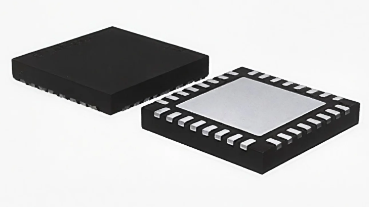
The Quad Flat Non-Lead Frame (QFN) package is a compact, surface-mount integrated circuit (IC) packaging technology designed for high-performance applications. It features a flat, leadless structure with metalized terminals at the bottom, allowing for direct electrical connection to the printed circuit board (PCB). The package typically includes an exposed die pad to enhance thermal dissipation, making it an efficient choice for heat-sensitive applications.
Compared to traditional IC packaging types such as Quad Flat Packages (QFP) and Dual In-Line Packages (DIP), the leadless package eliminates protruding leads, reducing parasitic inductance and improving electrical performance. Additionally, its low-profile design makes it ideal for space-constrained devices.
The Quad Flat Non-Lead Frame package is widely used in consumer electronics (smartphones, wearables, and laptops), automotive systems (advanced driver assistance systems, sensors, and infotainment modules), and industrial applications (IoT devices, power management systems, and communication modules). Its excellent electrical and thermal properties make it a preferred choice for modern, high-density electronic designs.
Lead Frame and Construction of Quad Flat Non-Lead Frame Packages
The Quad Flat Non-Lead Frame package is built on lead frame technology, a crucial foundation in semiconductor packaging that provides structural support and electrical connectivity for integrated circuits (ICs). Unlike traditional leaded packages, this package does not have protruding leads. Instead, it uses a flat metal lead frame with exposed terminals and a central die pad for efficient heat dissipation.
Key Components of the Quad Flat Non-Lead Frame Package
- Die Pad – The central metal pad serves as a mounting base for the semiconductor die and plays a critical role in thermal management by providing a direct heat dissipation path.
- Leads – Metalized contacts are positioned at the package’s perimeter but do not extend outward, allowing for a compact footprint and low electrical resistance.
- Encapsulation – A protective molding compound surrounds the die and leads, safeguarding the IC from environmental and mechanical stress.
Thermal and Electrical Performance Benefits
The Quad Flat Non-Lead Frame package excels in heat dissipation due to its exposed die pad, which enhances thermal conductivity by enabling direct contact with the PCB or an external heatsink. Additionally, the short interconnects reduce parasitic inductance and resistance, improving signal integrity and power efficiency. These features make it an optimal choice for high-performance applications in consumer electronics, automotive systems, and industrial devices.
Types of Quad Flat Non-Lead Frame Packages
The Quad Flat Non-Lead Frame (QFN) package comes in various types, each designed to meet specific application requirements. While all QFN variants share the core benefits of a leadless, surface-mount design, they differ in lead arrangement, thickness, and form factor. Understanding these differences is crucial for selecting the right package for a given application.
DFN (Dual Flat No-Lead) vs. QFN
The Quad Flat Non-Lead Frame package features a quad-sided lead arrangement, meaning its contact pads are distributed on all four sides of the package’s underside. In contrast, the Dual Flat No-Lead (DFN) package has a dual-sided lead configuration, with contact pads only on two opposite sides. This structural difference impacts routing flexibility and signal integrity.
- QFN Advantages: Superior electrical performance due to shorter interconnects and quad-sided contact distribution, making it ideal for high-frequency applications.
- DFN Advantages: Simpler PCB layout and cost-effectiveness for applications that do not require a quad-sided lead arrangement.
- Typical Applications: QFN is widely used in high-performance electronics such as microcontrollers and RF communication modules, while DFN is commonly found in power management ICs and sensors.
TDFN (Thin Dual Flat No-Lead) vs. QFN
The Thin Dual Flat No-Lead (TDFN) package is a variation of DFN with a reduced thickness, making it suitable for ultra-thin electronic devices. While the Quad Flat Non-Lead Frame package offers better thermal performance due to its larger die pad and quad-sided connectivity, TDFN is optimized for space-constrained applications.
- Key Difference: TDFN has a significantly lower profile than standard QFN, making it more suitable for wearables and compact medical devices.
- Application Scenarios: TDFN is preferred in ultra-thin consumer electronics such as fitness trackers, while QFN is used in high-performance processors and power modules.
VQFN (Very Thin Quad Flat No-Lead) vs. QFN
The Very Thin Quad Flat No-Lead (VQFN) package is a specialized version of the standard Quad Flat Non-Lead Frame package, designed with a significantly thinner profile. VQFN retains the quad-sided lead arrangement and exposed die pad for thermal efficiency but reduces the package height to accommodate space-constrained designs.
- Main Difference: VQFN has the same footprint as standard QFN but with a much lower height, making it ideal for applications requiring both high performance and minimal thickness.
- Use Cases: VQFN is widely used in high-density mobile devices, advanced sensors, and miniaturized automotive electronics, where vertical space is a critical design factor.
Each variation of the leadless flat package offers unique benefits, allowing designers to select the most suitable type based on space constraints, thermal requirements, and electrical performance needs.
Advantages of Quad Flat Non-Lead Frame Packaging
The Quad Flat Non-Lead Frame (QFN) package offers several key advantages that make it a preferred choice for modern electronic applications. Its unique structure, which eliminates protruding leads and features an exposed die pad, provides superior thermal and electrical performance while maintaining a compact form factor. These benefits contribute to the widespread adoption of QFN in consumer electronics, automotive systems, and industrial applications.
Improved Thermal Dissipation
One of the standout advantages of the Quad Flat Non-Lead Frame package is its excellent thermal performance. Unlike traditional leaded packages, QFN features an exposed die pad that provides a direct thermal path to the PCB. This design significantly enhances heat dissipation, reducing the risk of overheating and improving the reliability of high-power applications. By enabling efficient thermal transfer, QFN packages support higher-performance electronic components while minimizing the need for additional cooling solutions.
Better Electrical Performance with Shorter Interconnects
The Quad Flat Non-Lead Frame package improves electrical performance by reducing parasitic inductance and resistance. The absence of long leads results in shorter interconnects, which minimizes signal loss and enhances high-frequency performance. This makes QFN an ideal choice for RF applications, high-speed data transmission, and precision analog circuits. Compared to traditional leaded packages, QFN offers lower electrical noise and improved signal integrity, ensuring optimal performance in critical applications.
Reduced Package Size for High-Density PCB Design
The Quad Flat Non-Lead Frame package is designed to be compact and space-efficient, making it well-suited for high-density PCB layouts. With its leadless structure and minimal footprint, QFN allows designers to integrate more components onto a single PCB, supporting the development of smaller and more powerful electronic devices. This advantage is particularly valuable in mobile devices, IoT applications, and wearable technology, where space is a critical design constraint.
Cost-Effectiveness Compared to BGA and Other Advanced Packages
In addition to its technical advantages, the Quad Flat Non-Lead Frame package is also a cost-effective solution. Compared to Ball Grid Array (BGA) and other advanced packaging options, QFN has a simpler manufacturing process, reducing production costs. The absence of solder balls and complex underfill materials results in lower assembly expenses, making QFN a budget-friendly alternative for manufacturers without compromising on performance. Its compatibility with standard surface-mount technology (SMT) further simplifies production and reduces overall costs.
With its superior thermal and electrical characteristics, compact design, and cost-effectiveness, this package continues to be a leading choice for high-performance and space-constrained electronic applications.
Manufacturing and Assembly Process of Quad Flat Non-Lead Frame Packages
The Quad Flat Non-Lead Frame (QFN) package undergoes a precise manufacturing and assembly process to ensure high performance, reliability, and cost-effectiveness. From fabrication to PCB assembly, each step plays a crucial role in optimizing the electrical and thermal properties of the package. The combination of advanced semiconductor packaging techniques and Surface Mount Technology (SMT) enables this package to meet the stringent demands of modern electronic applications.
Steps in QFN Package Manufacturing
The manufacturing of the Quad Flat Non-Lead Frame package involves multiple steps to create a compact, high-performance package:
- Lead Frame Formation – A metal lead frame is fabricated from a copper alloy sheet, providing mechanical support and electrical pathways for the semiconductor die.
- Die Attach – The semiconductor die is attached to the central die pad using conductive adhesive or solder, ensuring strong mechanical bonding and efficient heat dissipation.
- Wire Bonding – Thin gold or copper wires connect the die to the lead frame, forming electrical connections between the chip and external circuits.
- Encapsulation – A molding compound encases the package, protecting the die and wire bonds from environmental factors such as moisture, dust, and mechanical stress.
- Lead Frame Etching/Plating – The exposed leads are chemically etched or plated with solderable materials such as tin, silver, or gold to enhance conductivity and solderability.
- Singulation – The packaged units are separated into individual components, typically through a mechanical sawing or laser-cutting process.
- Final Testing and Inspection – Electrical and mechanical tests are conducted to verify package integrity, performance, and compliance with quality standards before shipment.
SMT (Surface Mount Technology) Process for PCB Assembly
Once manufactured, the Quad Flat Non-Lead Frame package is mounted onto a PCB using SMT, a widely used technique for assembling miniaturized electronic components:
- PCB Preparation – A solder paste containing flux and metal particles is applied to the PCB’s copper pads using a stencil.
- Component Placement – The leadless package is precisely positioned on the PCB using automated pick-and-place machines.
- Reflow Soldering – The assembled PCB is heated in a reflow oven, melting the solder paste and creating strong electrical and mechanical bonds between the QFN package and the PCB.
- Inspection and Quality Control – Optical and X-ray inspections check for solder joint integrity, ensuring no defects such as voids, misalignment, or cold solder joints.
Considerations for Soldering and Reflow
Proper soldering techniques are essential to maximize the performance and reliability of the Quad Flat Non-Lead Frame package. Key considerations include:
- Solder Paste Selection – Using high-quality solder paste ensures strong adhesion and prevents issues like insufficient wetting or solder balling.
- Reflow Profile Optimization – A carefully controlled reflow temperature profile prevents overheating and ensures uniform solder joint formation.
- Void Reduction Strategies – Since QFN packages rely on their exposed die pad for heat dissipation, minimizing voids in the solder joint improves thermal performance.
- Inspection and Rework Challenges – Due to the leadless design, inspecting QFN solder joints requires X-ray imaging, and rework can be challenging without specialized equipment.
By following these meticulous manufacturing and assembly processes, the Quad Flat Non-Lead Frame package achieves superior electrical performance, thermal efficiency, and reliability, making it an optimal choice for modern electronic applications.
Common Challenges and Solutions in Quad Flat Non-Lead Frame Packaging
While the Quad Flat Non-Lead Frame (QFN) package offers significant advantages in modern electronics, its unique design presents several challenges during the soldering, assembly, and inspection processes. Addressing these issues is crucial to ensuring reliable performance and long-term durability. The most common challenges include soldering defects, thermal management concerns, and difficulties in inspection and rework.
Soldering Issues: Voiding, Wetting, and Misalignment
Proper soldering is essential for the Quad Flat Non-Lead Frame package, as poor solder joints can lead to electrical failures and reduced thermal performance.
-
Voiding in Solder Joints
- Challenge: The large exposed die pad at the bottom of the package often traps air, leading to void formation within the solder joint. These voids reduce thermal conductivity, affecting heat dissipation.
- Solution: Implementing optimized stencil designs with multiple smaller apertures for the solder paste, using vacuum-assisted reflow soldering, and controlling reflow profiles can significantly reduce voiding.
-
Poor Wetting and Cold Solder Joints
- Challenge: Insufficient solder paste volume or improper reflow temperatures can cause incomplete wetting, leading to weak or unreliable connections.
- Solution: Using high-quality solder paste, ensuring accurate stencil thickness, and optimizing the reflow profile with controlled ramp-up and cooling rates can improve solder wetting.
-
Misalignment During Placement
- Challenge: Since the Quad Flat Non-Lead Frame package has no visible leads, improper placement on the PCB can result in electrical disconnections or short circuits.
- Solution: Automated pick-and-place machines with high-precision vision alignment systems, along with fiducial markers on the PCB, help ensure accurate placement.
Thermal Management Challenges
Effective heat dissipation is critical for the Quad Flat Non-Lead Frame package, as overheating can degrade performance and reduce the lifespan of the IC.
- Challenge: Since the QFN package relies on its exposed die pad for heat dissipation, poor soldering or excessive voiding can impede thermal transfer, leading to overheating in high-power applications.
- Solution:
- Design PCBs with large copper-filled thermal vias under the exposed pad to enhance heat dissipation.
- Use thermal interface materials (TIM) or heat sinks for applications requiring superior cooling performance.
- Optimize the reflow soldering process to ensure a solid thermal connection between the exposed pad and the PCB.
Inspection and Rework Techniques
Unlike traditional leaded packages, the Quad Flat Non-Lead Frame package has hidden solder joints, making visual inspection and rework more challenging.
-
Difficulties in Optical Inspection
- Challenge: Since all solder joints are beneath the package, traditional optical inspection methods are ineffective.
- Solution: X-ray inspection is the most effective method for detecting soldering defects, such as voids, insufficient solder, or bridging under the package.
-
Rework and Repair Complexity
- Challenge: Removing and resoldering a Quad Flat Non-Lead Frame package without damaging nearby components is difficult due to its leadless design.
- Solution: Specialized rework stations with controlled infrared (IR) heating or hot air reflow can safely remove and replace QFN packages. Using flux and precise solder paste application ensures reliable reattachment.
By addressing these challenges with optimized manufacturing processes, precise thermal management strategies, and advanced inspection techniques, the Quad Flat Non-Lead Frame package can achieve high reliability and performance across various applications.
Applications and Future Trends of Quad Flat Non-Lead Frame Packaging
The Quad Flat Non-Lead Frame (QFN) package has become an essential component in modern electronics, playing a crucial role in applications ranging from consumer devices to advanced computing systems. As industries move towards more compact, power-efficient, and high-performance solutions, the demand for this packaging continues to grow. With its excellent thermal and electrical properties, QFN is widely used in cutting-edge technologies such as IoT, 5G, and AI-driven electronics. Moreover, advancements in semiconductor packaging are pushing the limits of QFN technology, making it even smaller, more efficient, and environmentally sustainable.
QFN’s Role in IoT, 5G, and AI-Driven Electronics
The rapid expansion of IoT, 5G, and artificial intelligence (AI) applications has significantly increased the adoption of Quad Flat Non-Lead Frame packages:
- IoT Devices: The miniaturized size and low power consumption of QFN packages make them ideal for IoT sensors, wearable technology, and smart home devices. Their ability to provide high-density integration supports the growing need for ultra-compact designs.
- 5G Infrastructure and Wireless Communication: The superior electrical performance of QFN, with minimal parasitic effects and low signal loss, makes it a preferred choice for RF applications in 5G base stations, wireless routers, and mobile communication systems.
- AI and High-Performance Computing: As AI-driven applications require faster processing and efficient power management, Quad Flat Non-Lead Frame packaging is increasingly used in AI accelerators, edge computing devices, and embedded systems where high-speed data processing is critical.
Advances in QFN Technology: Smaller and Higher-Performance Versions
The continuous evolution of Quad Flat Non-Lead Frame technology has led to the development of more advanced versions, improving performance while reducing footprint:
- Ultra-Thin QFN (VQFN and TDFN): These variants reduce overall package height, enabling even more compact device designs, particularly for mobile and portable electronics.
- Enhanced Thermal Management: Innovations in heat dissipation techniques, such as integrated heat spreaders and improved die attach materials, allow QFN packages to handle higher power loads while maintaining thermal stability.
- Higher Pin Count and Multi-Chip Integration: New QFN designs support higher pin densities and multi-chip integration, enabling more complex circuit designs within a single package.
Sustainability and Environmental Impact
With increasing focus on sustainability, Quad Flat Non-Lead Frame packaging is evolving to minimize environmental impact:
- Lead-Free and Halogen-Free Materials: Manufacturers are shifting towards eco-friendly materials, reducing hazardous substances while maintaining high-performance characteristics.
- Energy-Efficient Manufacturing: Advances in semiconductor fabrication have led to lower power consumption during the manufacturing process, reducing carbon footprints.
- Recyclability and Waste Reduction: The leadless design of QFN results in less material waste compared to traditional leaded packages, supporting greener electronics production.
As technology continues to advance, the Quad Flat Non-Lead Frame package will remain a critical solution for high-performance, energy-efficient, and environmentally sustainable electronics. Its adaptability to emerging trends in IoT, 5G, and AI-driven applications ensures that QFN packaging will play a central role in shaping the future of semiconductor technology.
FQAs Abut Quad Flat Non-Lead Frame
What is the quad flat no-lead package used for?
The Quad Flat No-Lead (QFN) package is primarily used for integrated circuits (ICs) in a variety of electronic devices. It is particularly favored for its excellent thermal performance, compact size, and high-density pin connections. Common applications include consumer electronics, automotive systems, industrial devices, wireless communication modules, and more. Its leadless design, with electrical contacts on the bottom of the package, makes it ideal for modern, space-constrained electronics, providing efficient performance in power-sensitive and high-speed applications.
What is the difference between DFN and QFN?
The primary difference between DFN (Dual Flat No-Lead) and QFN (Quad Flat No-Lead) is the number of leads. A DFN package has leads on two sides of the package, while a QFN package has leads on all four sides. This difference in lead arrangement affects the electrical and mechanical properties, as the QFN typically offers better robustness in terms of pin count and can handle higher pin density for more complex ICs. DFN packages are often used in smaller, lower-pin-count devices.
What is the difference between QFN and TDFN?
TDFN (Thin Dual Flat No-Lead) is a variation of the DFN package, with the main difference being the thickness of the package. TDFN is a thinner version of the DFN package, providing a more compact and low-profile solution for applications where space is extremely limited. While both have leads on two sides, the TDFN offers a slimmer form factor, making it suitable for applications requiring low height, such as mobile devices or portable electronics.
What is the difference between QFN and VQFN?
VQFN (Very Thin Quad Flat No-Lead) is a thinner and more compact version of the QFN package. The VQFN is designed with a reduced height, providing a more low-profile solution while maintaining the same lead configuration on all four sides as the standard QFN. This thinner version of QFN is typically used for applications where both a low profile and a higher level of thermal performance are needed, such as in modern smartphones, wearables, and high-performance computing devices.

