
Key Differences in QFN/QFP Lead Frame Packages
Integrated Circuit (IC) packaging is a crucial aspect of PCB (Printed Circuit Board) design, as it directly impacts the performance, reliability, and size of electronic devices. Different IC packages are designed to meet the diverse requirements of modern electronics, ranging from compact mobile devices to high-performance computing systems. Among the various packaging options, QFN/QFP Lead Frame packages have become increasingly popular due to their unique design features and advantages.
Understanding the differences between these two packages—QFN (Quad Flat No-lead) and QFP (Quad Flat Package)—is essential for engineers and designers. Both packages offer distinct electrical, mechanical, and thermal properties, making them suitable for different applications. This article will delve into the key differences, applications, and advantages of QFN/QFP Lead Frame packages, helping readers make informed decisions about which package best suits their design needs.
What is QFN (Quad Flat No-lead) Packaging? – A Key Component of QFN/QFP Lead Frame
QFN (Quad Flat No-lead) packaging is a popular type of surface-mount IC package that offers a flat and compact design, making it ideal for space-constrained applications. As the name suggests, QFN packages feature no leads on the sides of the package, unlike traditional IC packages such as QFP (Quad Flat Package). Instead, the leads are located underneath the package, which allows for a cleaner, more compact footprint on the PCB. This design reduces the overall height of the component, making it suitable for slim and lightweight devices.
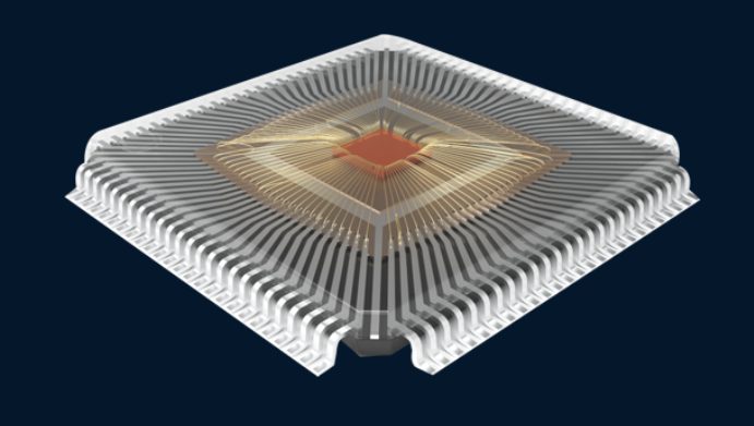
The QFN/QFP Lead Frame forms the core structure of the QFN package, with metal leads embedded in the frame, connecting the IC to the PCB. This lead frame is precisely designed and molded to support the IC and ensure efficient electrical connections. The leads in a QFN package are typically arranged in a grid pattern underneath the component, which not only minimizes the overall height but also optimizes thermal management.
QFN packages are widely used in industries such as automotive, telecommunications, and consumer electronics. Their small footprint and efficient performance make them ideal for applications that require high-density components, such as microcontrollers, power management ICs, and sensors.
Advantages of QFN Packaging
QFN packaging offers several key advantages that make it an attractive option for modern electronics:
- High Density: Due to its compact design, QFN packages can accommodate a large number of pins in a small space, making it ideal for high-density applications.
- Lower Profile: The flat structure allows for a much lower profile compared to other packages, making it easier to integrate into smaller devices.
- Better Thermal Performance: The leads are placed underneath the package, improving heat dissipation and enhancing thermal management, which is critical for high-power applications.
- Signal Integrity: The short lead lengths and direct connection to the PCB help to maintain signal integrity, especially for high-frequency circuits, reducing the risk of electromagnetic interference (EMI).
Overall, QFN/QFP Lead Frame packaging offers a robust solution for designs that require compactness, improved heat dissipation, and high-performance electrical characteristics.
What is QFP (Quad Flat Package) Packaging? – Part of the QFN/QFP Lead Frame Family
QFP (Quad Flat Package) is another popular IC package type, characterized by leads on all four sides of the package. Unlike QFN (Quad Flat No-lead) packages, which have leads underneath, QFP packages extend leads outward from the edges of the component. These leads are typically arranged in rows along each side of the package, providing a clear path for electrical connections to the PCB. This design makes QFP packages relatively easy to handle and assemble, especially in through-hole or surface-mount configurations.
As part of the QFN/QFP Lead Frame family, the QFP package shares similarities with QFN, but the key difference lies in the placement of the leads. QFP packages tend to have a larger footprint compared to QFN packages, which makes them less ideal for compact designs but more suitable for applications where size is not as critical.
Key Features of QFP Packaging
- Leads on All Four Sides: QFP packages are known for their side leads, which are positioned on each of the four sides of the package. This makes it easier to solder and mount compared to no-lead packages like QFN.
- Larger Footprint: Typically, QFP packages require more space than QFN packages because of the outward-facing leads. However, this larger footprint can be advantageous when dealing with components that need more pins or require more space for proper thermal management.
- Soldering and Assembly: QFP packages are easier to assemble and solder, especially with automated processes like wave soldering. The exposed leads on the sides are more accessible for traditional soldering techniques compared to the leads under a QFN package.
Key Applications of QFP
QFP packages are used in various applications that require high pin counts, such as:
- Microcontrollers: Often used in embedded systems where a large number of I/O pins are required.
- Signal Processors: Ideal for signal processing ICs in telecommunications, automotive systems, and consumer electronics.
- Networking Equipment: Used in network processors and controllers, where high-speed data transfer and multiple input/output connections are crucial.
Advantages of QFP Packaging
QFP packages offer several advantages, particularly in applications where higher pin counts and ease of assembly are important:
- Easy Soldering: The leads on the sides of the package make QFP packages easier to solder using traditional methods, such as wave soldering, compared to QFN packages, which require more advanced reflow techniques.
- Higher Pin Count: QFP packages typically support a larger number of pins compared to many other surface-mount packages, which makes them ideal for applications requiring complex connectivity.
- Better Thermal Management: The side leads of QFP packages allow for more effective heat dissipation when compared to packages with leads underneath, providing a more stable thermal environment for the IC.
While QFN/QFP Lead Frame packages differ in design and functionality, QFP’s easy-to-handle leads and larger footprint make it an excellent choice for applications that demand a higher number of connections and simpler assembly processes.
QFN vs. QFP: Key Differences in the QFN/QFP Lead Frame Packaging
When comparing QFN (Quad Flat No-lead) and QFP (Quad Flat Package) packaging, it’s important to understand the core differences in their design, functionality, and performance. Both packages belong to the QFN/QFP Lead Frame family, but they are optimized for different applications based on their unique features. Below are the key differences between QFN and QFP packages.
Pin Configuration in QFN/QFP Lead Frame Packages
The most noticeable difference between QFN and QFP packages lies in their pin configuration. In QFN/QFP Lead Frame packaging, QFP features leads that extend from all four sides of the package. These side leads make it easier for traditional soldering techniques like wave soldering. On the other hand, QFN has no visible leads on the sides. Instead, it features pads underneath the package, making it a leadless design. These pads connect to the PCB via soldering during the assembly process, requiring more advanced reflow soldering techniques.
QFN/QFP Lead Frame: Profile & Size Differences
One of the primary distinctions between QFN and QFP packages is their profile and size. QFN/QFP Lead Frame packages are available in various sizes, but generally, QFN packages offer a significantly smaller profile compared to QFP. This compact size makes QFN ideal for designs that require space-saving solutions, such as mobile phones, wearables, and IoT devices. In contrast, QFP packages tend to be bulkier, which makes them suitable for applications where the footprint is less of a concern, and there’s more room for components, such as in desktop electronics or networking hardware.
Thermal Performance
QFN packages typically offer better thermal performance compared to QFP. This advantage stems from the design of QFN/QFP Lead Frame packages, where the leads in QFN packages are positioned directly beneath the component. This configuration allows heat to dissipate more efficiently through the PCB, providing better thermal management, especially in power-intensive applications. The thermal performance is crucial in preventing overheating and ensuring the long-term reliability of the device. QFP, with its side leads, may not provide the same level of thermal conductivity due to the less direct path for heat dissipation.
Assembly & Soldering
When it comes to assembly and soldering, QFN/QFP Lead Frame packages differ significantly. QFP packages are easier to assemble using traditional wave soldering methods because the leads are exposed on the sides, making them accessible for the soldering process. QFP packages are also more forgiving during manual soldering. In contrast, QFN packages require more advanced assembly methods like reflow soldering. Since QFN leads are located under the package, the assembly process demands precise control of the reflow soldering to ensure proper bonding between the pads and the PCB.
Electrical Performance
From an electrical performance perspective, QFN packages generally outperform QFP packages, especially for high-frequency applications. This is because QFN/QFP Lead Frame packages provide shorter electrical paths due to the leads being directly under the package, which helps reduce signal interference and loss. The small size and low inductance of QFN packages make them ideal for applications requiring high-speed signal transmission, such as RF (radio frequency) circuits and high-frequency data processing. QFP packages, while suitable for general-purpose applications, tend to have longer electrical paths, which can lead to higher inductance and reduced signal integrity in high-frequency circuits.
QFN/QFP Lead Frame packages each have distinct advantages depending on the application. QFN packages are ideal for compact designs that require better thermal management, high-frequency performance, and space efficiency. On the other hand, QFP packages are more suitable for applications where ease of assembly, higher pin count, and traditional soldering techniques are prioritized. Understanding these differences is crucial for selecting the appropriate packaging solution for your PCB design needs.
QFN vs. Leaded Packages: Understanding the Differences in QFN/QFP Lead Frame Packaging
Leaded packages, which include both through-hole and surface-mount varieties, are some of the most traditional and widely used IC packaging types in the electronics industry. These packages have pins that extend from the sides of the component, allowing them to be soldered either through holes in the PCB (through-hole packages) or directly onto the surface (surface-mount packages). In contrast, QFN/QFP Lead Frame packages, such as QFN (Quad Flat No-lead) and QFP (Quad Flat Package), have a different design that eliminates the need for side leads, offering a more compact and efficient solution in many modern designs.
Definition of Leaded Packages
Leaded packages are ICs that feature metal pins extending outward from the sides of the package. These pins provide the electrical connections between the IC and the PCB. Leaded packages are commonly used in both through-hole technology (where the leads pass through the PCB) and surface-mount technology (where the leads are soldered directly to the PCB surface). Examples of leaded packages include the widely used DIP (Dual In-line Package), SOIC (Small Outline Integrated Circuit), and TSSOP (Thin Shrink Small Outline Package).
In QFN/QFP Lead Frame packaging, the leads are arranged differently. QFP packages have leads on all four sides of the component, while QFN packages have no visible leads but rather pads beneath the package for soldering. This key difference affects both the mechanical and electrical properties of the packages.
Comparison of Electrical, Mechanical, and Thermal Properties
-
Electrical Properties:
- Leaded packages generally have longer lead lengths compared to QFN/QFP Lead Frame packages. These longer leads can introduce higher inductance, which may affect signal integrity, especially in high-frequency circuits. This is because longer leads increase the resistance and inductance, making them less suitable for high-speed or high-frequency applications.
- QFN packages, with their leads placed underneath the package, have shorter electrical paths, which helps to maintain better signal integrity and lower inductance. The minimized lead length is especially beneficial for high-frequency and RF (radio frequency) applications where signal integrity is critical.
-
Mechanical Properties:
- Leaded packages tend to be mechanically stronger due to the extended leads, which can provide more secure connections when using traditional soldering techniques. However, the mechanical reliability of these packages can be influenced by the type of soldering method (wave soldering for through-hole or reflow soldering for surface-mount).
- QFN/QFP Lead Frame packages, particularly QFN, are more compact and robust due to their low-profile design, making them ideal for smaller, space-constrained applications. The absence of leads extending from the sides reduces the overall package height, which is advantageous for designs where height is a critical factor.
-
Thermal Properties:
- Leaded packages generally have less efficient thermal management compared to QFN/QFP Lead Frame packages. The leads of leaded packages are positioned around the periphery, which can reduce the efficiency of heat dissipation. Moreover, the larger physical size of leaded packages often means they have more thermal resistance.
- QFN packages, on the other hand, provide superior thermal performance. The leads are directly under the package, which facilitates better heat conduction through the PCB, improving heat dissipation. This makes QFN packages a better choice for high-power applications where thermal management is crucial.
Advantages of QFN over Leaded Packages
QFN/QFP Lead Frame packages offer several advantages over traditional leaded packages:
- Better Performance in Compact Designs: The QFN/QFP Lead Frame design, especially QFN, is well-suited for space-saving applications. Its low-profile design allows for smaller and thinner products, such as mobile devices, wearables, and compact automotive systems.
- Improved Thermal Management: QFN packages provide superior heat dissipation compared to leaded packages, thanks to the leads being positioned directly underneath the component. This feature is particularly beneficial for power management ICs and other heat-sensitive components.
- Reduced Electromagnetic Interference (EMI): QFN packages have shorter leads, which helps reduce the electromagnetic interference (EMI) caused by longer leads in traditional leaded packages. This makes QFN ideal for high-frequency applications, such as RF circuits, where minimizing signal loss and interference is critical.
Applications for Leaded Packages
Despite the many advantages of QFN/QFP Lead Frame packaging, leaded packages are still widely used in specific applications where certain factors are prioritized:
- Ease of Manual Soldering: Leaded packages are easier to solder manually, which makes them ideal for prototyping or low-volume production where automated assembly may not be practical.
- Durability in Harsh Environments: Leaded packages can be more robust in environments where mechanical stresses and vibrations are a concern, such as in automotive or industrial applications.
- Through-Hole Technology: For certain designs, especially those that require very strong mechanical connections, leaded packages using through-hole technology are preferred. This is often the case for components that must be physically secure or for designs requiring high-pinning-count packages.
While QFN/QFP Lead Frame packages are increasingly preferred in modern electronics due to their smaller size, better thermal performance, and superior electrical characteristics, leaded packages remain valuable in applications where manual assembly, mechanical durability, or through-hole technology is required. Understanding the unique advantages and limitations of each type is key to selecting the right package for a given application.
QFN vs. BGA (Ball Grid Array): Key Differences in QFN/QFP Lead Frame Packaging
Ball Grid Array (BGA) is another advanced IC packaging technology that shares similarities with QFN/QFP Lead Frame packages but has distinct advantages when it comes to high-performance, high-density applications. BGA and QFN are both surface-mount packages, but their design, structure, and suitable applications differ considerably. In this section, we’ll explore the differences between QFN and BGA packaging, as well as the strengths of each.
Definition and Structure of BGA Packaging
BGA (Ball Grid Array) packaging is a type of surface-mount package where the electrical connections between the IC and the PCB are made using solder balls arranged in a grid pattern on the underside of the package. These solder balls serve as both the leads and the connection points, allowing for high-density interconnects. BGA packaging has become increasingly popular for high-performance applications due to its excellent electrical and thermal properties.
Unlike QFN/QFP Lead Frame packages, where the leads are positioned under the component in a pad-like fashion, BGA’s solder balls are spread in a grid layout. This design allows for a higher number of pins and a more efficient use of PCB space, enabling greater pin density in smaller package sizes. BGA packages typically have larger footprints compared to QFN but are still compact when considering the number of connections they offer.
Comparison with QFN
While both QFN and BGA packages are used for surface-mount applications, there are some key distinctions between the two:
-
Pin Count:
- BGA is more suitable for higher pin-count ICs. Because BGA uses a grid of solder balls, it can accommodate many more connections than a QFN/QFP Lead Frame package. This makes BGA ideal for applications requiring a high number of input/output connections, such as microprocessors, FPGAs, and other high-density components.
- QFN, on the other hand, is typically better suited for lower-pin-count ICs. While QFN can still offer a relatively high number of pins, it is usually used for less complex components where space is critical, and the design doesn’t require the massive pin count that BGA can provide.
-
Package Size:
- BGA packages often have a larger footprint compared to QFN because they are designed to accommodate many more pins. However, the BGA design maximizes the number of pins per unit area, which can be an advantage when dealing with high-performance components.
- QFN packages are typically smaller and more compact, making them ideal for space-constrained applications. The small size of QFN allows for more efficient use of board real estate, which is important in portable or handheld devices.
Key Differences
There are several fundamental differences between QFN/QFP Lead Frame packages and BGA, particularly regarding electrical and thermal performance, as well as the assembly process:
-
Electrical and Thermal Performance:
- BGA offers superior electrical and thermal performance compared to QFN due to its direct connection to the PCB through the solder balls. This connection provides a low-resistance path for electrical signals, which is essential for high-speed circuits. Additionally, the larger surface area for solder balls in BGA packages enables better heat dissipation, making it an excellent choice for power-hungry components.
- QFN, while still offering good thermal management due to its lead frame design, generally has a lower number of connections and is typically used in applications where thermal performance is important but not as critical as in high-performance processors or FPGAs.
-
Assembly Techniques:
- BGA requires precise assembly methods, especially reflow soldering. The solder balls need to be melted at high temperatures in a controlled process to ensure that the IC is securely attached to the PCB. This requires specialized equipment for precise alignment and soldering, making BGA assembly more challenging than that of QFN/QFP Lead Frame packages.
- QFN, in comparison, is easier to handle during assembly, especially with its simpler reflow soldering process, as the leads are placed directly underneath the component. While QFN still requires careful soldering, it does not demand the level of precision required by BGA.
Applications
The differences between QFN/QFP Lead Frame and BGA packaging lead to distinct use cases for each type:
-
BGA Applications: BGA packaging is commonly used in high-performance, high-density designs such as:
- Microprocessors: These require high pin-count connections for fast data processing and low power consumption.
- FPGAs (Field-Programmable Gate Arrays): FPGAs demand high-speed signal transmission and a large number of I/O pins, which makes BGA the preferred packaging choice.
- Graphics Processors: GPUs, which require high bandwidth and low-latency communication, benefit from the superior electrical performance of BGA packages.
- Networking Equipment: BGA is also used in advanced networking equipment, such as routers and switches, which demand high pin counts and thermal efficiency.
-
QFN Applications: QFN/QFP Lead Frame packages, on the other hand, are often used in applications where space constraints are critical but pin count is lower:
- Power Management ICs: Due to their compact size and good thermal properties, QFN is commonly used for power management ICs in smartphones, wearables, and other portable devices.
- Sensor ICs: Many sensors used in automotive, consumer electronics, and IoT devices benefit from the compact nature of QFN.
- Microcontrollers: For applications requiring a moderate number of pins, QFN offers a space-efficient solution.
Both QFN/QFP Lead Frame packages and BGA packaging have their place in modern electronics, but their suitability depends largely on the specific application requirements. BGA is ideal for high-performance, high-density designs where electrical and thermal performance are critical, and where a large number of pins are needed. QFN, on the other hand, is better suited for space-constrained applications, offering a smaller profile and simpler assembly, but typically supporting fewer pins. Understanding these differences will help engineers choose the most appropriate package for their specific design needs.
What is WCSP (Wafer-Level Chip-Scale Package)? – Part of the QFN/QFP Lead Frame Family
The Wafer-Level Chip-Scale Package (WCSP) is a modern IC packaging solution that shares similarities with QFN/QFP Lead Frame packages but offers even smaller form factors, making it ideal for ultra-compact devices. WCSPs are created directly at the wafer level, before the individual ICs are diced, resulting in smaller, more efficient packages that are used in applications where size and performance are crucial. In this section, we will explore the definition, structure, and advantages of WCSP, as well as how it compares to QFN/QFP Lead Frame packages.
Definition of WCSP
A Wafer-Level Chip-Scale Package (WCSP) is a type of semiconductor package where the package is formed directly on the wafer during the manufacturing process, rather than being assembled after the die is separated. This method results in a package that is nearly the same size as the semiconductor die itself, typically offering a very small form factor. Like QFN/QFP Lead Frame packages, WCSP uses small solder pads or balls that connect the IC to the PCB, allowing for surface-mount assembly.
The wafer-level approach provides several advantages, including the ability to create packages with minimal space between the die and the PCB. This level of miniaturization is particularly beneficial in applications where reducing size is a priority, such as in mobile devices, wearables, and IoT (Internet of Things) products.
Comparison with QFN
While both WCSP and QFN/QFP Lead Frame packages are designed for compactness and efficient use of space, there are key differences between the two:
-
Profile and Size:
- WCSP is even smaller than QFN. Since it is created directly on the wafer, it can achieve a package size that is almost identical to the die itself, making WCSP extremely compact. This smaller profile allows for even greater miniaturization, which is ideal for ultra-small form-factor applications.
- QFN packages, although low-profile and compact, generally take up more space than WCSP packages because of the additional lead frame and the need for under-package leads. QFN is still an excellent choice for small designs but doesn’t reach the extreme miniaturization that WCSP offers.
-
Assembly:
- WCSP typically uses solder balls, similar to the BGA or QFN designs, but the soldering process is done at the wafer level, resulting in a more seamless integration into the PCB. This is different from QFN, where leads are placed under the package and require precise reflow soldering methods.
- QFN has a simple soldering process but may not be as efficient for extreme miniaturization, especially in mobile or wearable devices where every millimeter counts.
Advantages of WCSP
WCSP packaging offers several key advantages, particularly in applications where size and performance are critical:
-
Smaller Size: The most notable advantage of WCSP is its tiny form factor. Since the package is created directly on the wafer and is nearly the same size as the die, it is ideal for devices that demand ultra-small components, such as mobile phones, smartwatches, and wearable electronics. This extremely compact design minimizes the footprint and reduces the overall size of the device.
-
Ideal for Consumer Electronics: WCSP is particularly well-suited for consumer electronics where size constraints are a major consideration. For products like smartphones, wearables, and IoT devices, space is limited, and WCSP’s small profile allows manufacturers to pack more functionality into less space without sacrificing performance.
-
Improved Electrical and Thermal Performance: Like QFN/QFP Lead Frame packages, WCSPs provide excellent thermal and electrical performance. Due to the proximity of the package to the PCB, WCSPs benefit from shorter interconnects and better heat dissipation, which is crucial for high-performance components that generate heat during operation. The small size and direct contact between the solder balls and the PCB also enhance the overall performance of the device.
Applications of WCSP
WCSP is widely used in applications that require the highest degree of miniaturization, including:
- Mobile Devices: With the increasing demand for smaller smartphones, tablets, and other portable gadgets, WCSPs are used to package components like sensors, power management ICs, and memory modules.
- Wearables: Smartwatches, fitness trackers, and other wearables require ultra-small IC packages, and WCSP is ideal for providing the necessary functionality in these compact devices.
- IoT Devices: Internet of Things (IoT) applications often need small, low-power ICs to fit into tight spaces. WCSP offers a space-efficient solution for these devices, which may be embedded in everything from home appliances to medical devices.
In the realm of QFN/QFP Lead Frame packaging, WCSP offers an innovative solution for applications that demand the smallest possible form factors without compromising on performance. Its wafer-level assembly process and tiny package size make it perfect for consumer electronics, wearables, and IoT devices. By offering significant size reduction, WCSP is poised to play a crucial role in the future of compact and high-performance electronics, providing a competitive edge in applications where space is at a premium.
Lead Frame Technology: The Backbone of QFN/QFP Lead Frame Packaging
Lead frame technology plays a crucial role in the manufacturing of QFN/QFP Lead Frame packages. It forms the essential structure that connects the Integrated Circuit (IC) to the Printed Circuit Board (PCB) through leads, providing both electrical and mechanical stability. This section will delve into the details of lead frame technology, including the manufacturing process, material considerations, and different types of lead frames used in various packages.
Explanation of Lead Frame Technology
At the heart of QFN/QFP Lead Frame packages lies the lead frame, a metal structure that serves as the foundation for the IC. The lead frame is responsible for providing the electrical connections from the IC’s internal circuitry to the external PCB. The frame supports the IC chip and forms the leads that connect to the PCB’s surface-mount pads (in the case of QFN) or to the pins extending from the sides of the package (in the case of QFP).
In QFN/QFP Lead Frame packages, the lead frame is typically located at the bottom of the IC, forming a network of electrical paths. For QFN, the leads are underneath the package, while for QFP, the leads extend outward from the four sides. The lead frame thus provides the mechanical integrity needed for the IC to stay securely in place while ensuring reliable electrical conduction.
The structure of the lead frame ensures that the IC can be assembled efficiently and that the electrical connections remain stable over time, even under various environmental stresses. The lead frame is designed to accommodate the number of leads required by the IC while also ensuring thermal management, as the frame helps dissipate heat away from the IC.
Manufacturing Process of Lead Frames
The manufacturing of lead frames is a multi-step process that involves various techniques to ensure precision, durability, and reliability. The main steps in the lead frame manufacturing process include:
-
Stamping: This is the first step in the creation of lead frames. A metal strip, usually made of copper or another conductive material, is fed into a stamping machine, where it is precisely cut into the desired shape. The process involves cutting the lead frame to form the leads and the frame that will surround the IC chip. During this process, various features such as die pads and lead segments are formed.
-
Etching: After the initial stamping, the lead frame is etched to remove excess material and refine the lead structure. Etching is typically used to form fine patterns and ensure that the leads are precisely shaped to align with the IC’s electrical connections. This process can also be used to add any additional features or markings to the lead frame, such as electrical traces or guide pins.
-
Molding: Once the lead frame is prepared, it is subjected to molding, where it is encapsulated in a plastic or resin compound. This encapsulation helps protect the IC and its delicate leads from external damage while providing the necessary insulation. In QFN/QFP Lead Frame packaging, the molding process is crucial for maintaining the integrity of the IC and ensuring that the leads remain securely attached to the frame.
Material Considerations for Lead Frames
The choice of material for the lead frame is critical, as it affects both the electrical and thermal performance of the IC package. The most common material used for lead frames in QFN/QFP Lead Frame packages is copper, due to its excellent electrical and thermal conductivity. Copper helps ensure that the electrical signals pass through the leads with minimal resistance and that heat is efficiently dissipated away from the IC.
Other materials used for lead frames may include:
- Copper Alloy: A common variant of copper, which is often used for lead frames requiring higher strength and durability.
- Copper-Clad Steel: This material is sometimes used for lead frames that require both electrical conductivity and strength, particularly in environments where mechanical stability is essential.
- Gold: While not as common as copper, gold can be used for lead frames in high-performance applications where superior electrical conductivity and corrosion resistance are required.
The material choice impacts not only the package’s performance but also its cost, as high-conductivity metals such as gold can increase the manufacturing expense. However, copper-based lead frames offer a good balance between performance, cost, and manufacturability.
Types of Lead Frames in QFN/QFP Lead Frame Packages
There are several types of lead frames used in QFN/QFP Lead Frame packaging, each designed to meet the specific needs of the IC and its application. The most common types of lead frames are:
-
Single-Row Lead Frame: This type of lead frame has a single row of leads extending from the IC package. It is commonly used in lower-pin-count packages, such as small QFN or QFP designs. Single-row lead frames are ideal for compact, low-pin-count devices that still require reliable electrical connections.
-
Double-Row Lead Frame: As the name suggests, a double-row lead frame has two parallel rows of leads. This type of lead frame is used for medium-pin-count ICs, where the package needs more connections but still requires a relatively simple structure. Double-row lead frames are common in devices like memory ICs and mid-range processors.
-
Multi-Row Lead Frame: Multi-row lead frames are designed for high-pin-count ICs, such as those found in complex processors or FPGA packages. These lead frames feature multiple rows of leads, typically arranged in a grid-like pattern to provide a dense and efficient connection interface. Multi-row lead frames are used in QFP packages with high-pinning counts, making them suitable for larger, more complex components.
Each of these lead frame types is carefully selected based on the specific needs of the IC, including the number of connections required, the size constraints, and the overall thermal and electrical performance requirements.
QFN/QFP Lead Frame technology is at the core of many modern IC packaging solutions, providing a robust structure for both electrical connections and mechanical stability. The manufacturing process, involving stamping, etching, and molding, ensures that the lead frame meets precise standards for performance and reliability. Material considerations, particularly the use of copper or copper alloys, help maintain excellent electrical and thermal properties, while the different types of lead frames cater to the varying needs of ICs, from small consumer electronics to complex processors. Understanding lead frame technology is essential for designing efficient, high-performance packages that meet the demands of today’s fast-evolving electronics industry.
Applications and Market Trends of QFN/QFP Lead Frame Packaging
The QFN/QFP Lead Frame packaging technology has found widespread adoption across various industries due to its versatility, compact design, and efficient thermal and electrical performance. As the demand for smaller, faster, and more reliable electronic devices continues to grow, the applications of QFN/QFP Lead Frame packages are becoming increasingly diverse. This section explores the common uses of these packages, the growing trend towards miniaturization, and future trends in lead frame technology.
Common Uses of QFN/QFP Lead Frame Packaging
QFN/QFP Lead Frame packages are integral to a broad range of industries due to their ability to offer compact, high-performance solutions for electronic components. Some of the most common applications include:
-
Automotive: Automotive electronics require packages that are durable, efficient, and able to withstand harsh environmental conditions. QFN/QFP Lead Frame packages are frequently used in automotive systems for power management ICs, sensors, microcontrollers, and communication devices. The small size and excellent thermal properties of QFN make it particularly valuable for automotive applications, where space and heat dissipation are critical considerations.
-
Telecommunications: In the telecommunications sector, QFN/QFP Lead Frame packages are commonly used in RF (Radio Frequency) components, base station equipment, and networking hardware. These packages help ensure that high-frequency signals are transmitted with minimal interference, thanks to their superior signal integrity and compact design. The small footprint of QFN packages is particularly beneficial in mobile devices, Wi-Fi routers, and other telecommunications equipment that demand high-speed data transmission in tight spaces.
-
Consumer Electronics: Consumer electronics, such as smartphones, tablets, wearables, and gaming devices, rely heavily on QFN/QFP Lead Frame packages for their small size, high pin-count, and excellent thermal performance. The demand for sleek, portable devices drives the use of QFN packages, which are commonly found in power management ICs, audio ICs, memory chips, and wireless communication components. QFP Lead Frame packages also play a key role in applications requiring medium to high pin-count ICs, such as display drivers and audio processing units.
-
Medical Devices: In medical devices, reliability, miniaturization, and precision are paramount. QFN/QFP Lead Frame packages are used in a variety of healthcare applications, including diagnostic equipment, patient monitoring systems, hearing aids, and medical sensors. The compact nature of QFN packages is well-suited for wearable medical devices and implants, where space is limited and high functionality is required. The ability of QFP to handle higher pin-counts makes it ideal for complex medical instrumentation.
The Growing Trend Towards Miniaturization
As consumer demand for smaller and more powerful devices continues to rise, miniaturization has become a driving force in the electronics industry. QFN/QFP Lead Frame packages are particularly well-suited to address this trend, especially QFN, which is gaining increasing popularity for space-constrained designs.
-
Space-Constrained Designs: QFN packages are prized for their low profile and compact size, which make them ideal for applications where board space is limited. As mobile devices, wearables, and IoT products become more compact, there is a growing need for smaller, higher-performing components. QFN’s compact form factor allows for efficient use of space, enabling manufacturers to pack more features into smaller devices without sacrificing performance.
-
Demand for Smaller Components: QFN is often preferred in designs that require ultra-small form factors, such as in the mobile device sector and in IoT devices. With features like smaller die sizes, lower profile heights, and minimal lead exposure, QFN packages are ideal for applications where size and power efficiency are critical. The trend towards miniaturization has been driven by consumer demands for sleeker, more functional electronics in smaller, more portable packages.
Future Trends in QFN/QFP Lead Frame Technology
As the electronics market evolves, several trends in QFN/QFP Lead Frame technology are emerging, pointing toward even more advanced packaging solutions. These advancements will continue to play a critical role in high-performance applications.
-
Advancements in Lead Frame Technology: The lead frame manufacturing process continues to evolve, with innovations aimed at improving the precision, reliability, and performance of QFN/QFP Lead Frame packages. As the demand for more complex ICs grows, new materials, like copper alloys and hybrid materials, are being explored to further improve the thermal and electrical properties of lead frames. Additionally, the manufacturing techniques for lead frames are becoming more advanced, allowing for finer, more intricate designs that can handle higher pin counts and more demanding performance criteria.
-
Emerging Packaging Solutions – 3D ICs: One of the most exciting developments in the world of semiconductor packaging is the rise of 3D ICs. 3D packaging involves stacking multiple ICs vertically, creating highly compact solutions with increased functionality. QFN/QFP Lead Frame packages will play a key role in 3D IC technologies, as they can serve as the base for these stacked IC structures, facilitating the connections between layers. The use of 3D packaging is particularly promising for applications requiring high performance in a small footprint, such as mobile devices, gaming consoles, and high-end computing equipment.
-
Role of QFN in High-Performance Applications: As devices become more powerful, QFN packages are poised to play an important role in high-performance applications that demand fast, efficient signal transmission, and heat management. For example, QFN is well-suited for processors, power amplifiers, and RF components in high-performance systems like 5G infrastructure, advanced automotive systems, and industrial automation. The demand for low-latency, high-speed performance in these sectors will drive continued innovation and adoption of QFN packaging.
The future of QFN/QFP Lead Frame packaging looks bright, with the technology continuing to evolve to meet the demands of ever-smaller, more powerful, and more efficient electronic devices. From automotive systems to consumer electronics, QFN/QFP Lead Frame packages are critical to the functionality and miniaturization of modern products. As lead frame technology advances and new packaging solutions like 3D ICs emerge, QFN and QFP will continue to be central to the development of high-performance, space-efficient electronic components for a wide range of applications.
FQAs Abut QFN/QFP Lead Frame
What is the difference between QFP and QFN?
-
Pin Configuration:
- QFP (Quad Flat Package) has leads on all four sides of the package.
- QFN (Quad Flat No-lead) has no visible leads; instead, it has pads underneath the package.
-
Size and Profile:
- QFP typically has a larger footprint and a higher profile compared to QFN.
- QFN is more compact and has a lower profile, making it ideal for space-constrained designs.
-
Thermal and Electrical Performance:
- QFN generally provides better thermal dissipation as its leads (pads) are located directly underneath the package, offering better heat transfer to the PCB.
- QFP has relatively less efficient thermal performance due to leads on the sides.
-
Assembly and Soldering:
- QFP is easier to assemble using traditional wave soldering methods.
- QFN requires more advanced assembly techniques, such as reflow soldering, due to the leads being underneath.
What is the difference between QFN and leaded packages?
-
Pin Configuration:
- Leaded packages have pins extending from the sides of the package (through-hole or surface-mount).
- QFN has no leads on the sides; it has pads underneath for soldering to the PCB.
-
Electrical and Thermal Performance:
- QFN packages provide superior thermal management because the pads are directly connected to the PCB, leading to better heat dissipation.
- Leaded packages tend to have less efficient thermal dissipation as their leads are positioned farther from the PCB.
-
Mechanical and Assembly:
- Leaded packages are easier to solder using traditional methods (wave or hand soldering).
- QFN requires more advanced techniques, like reflow soldering, for assembly due to its pad-only configuration.
-
Size and Profile:
- Leaded packages are typically bulkier and have a larger footprint.
- QFN has a smaller, more compact profile, which makes it better suited for space-constrained applications.
What is the difference between WCSP and QFN?
-
Package Type:
- WCSP (Wafer-Level Chip-Scale Package) is a package that is formed directly at the wafer level, often resulting in a smaller package size compared to QFN.
- QFN packages are typically formed after the wafer is diced, with leads or pads underneath the package.
-
Size and Profile:
- WCSP offers a smaller form factor, usually thinner than QFN.
- QFN has a slightly larger profile and is commonly used in applications that require a balance of size and performance.
-
Applications:
- WCSP is often used in applications that require ultra-small sizes, such as mobile devices or IoT applications.
- QFN is commonly used in power management, automotive, and telecommunications applications where heat dissipation and electrical performance are critical.
-
Assembly:
- WCSP uses solder balls on the underside, similar to BGA, which provides excellent electrical and thermal performance.
- QFN uses pads underneath for soldering, typically via reflow soldering methods.
What is the difference between BGA and QFN?
-
Pin Configuration:
- BGA (Ball Grid Array) has solder balls arranged in a grid pattern on the underside of the package.
- QFN has pads arranged underneath the package but does not use solder balls; it uses flat pads for surface mounting.
-
Pin Count:
- BGA is used for higher pin-count devices (often in the hundreds or thousands of pins).
- QFN is more commonly used for lower to moderate pin-count ICs.
-
Thermal and Electrical Performance:
- BGA provides superior electrical and thermal performance due to its direct connection of pins to the PCB via solder balls. The direct contact with the PCB offers better heat dissipation.
- QFN also offers good thermal performance but not as high as BGA in designs that require many pins and higher-density interconnections.
-
Assembly:
- BGA requires more advanced assembly techniques, including precise reflow soldering and often X-ray inspection for solder joint reliability.
- QFN also uses reflow soldering but is simpler to handle compared to BGA in terms of assembly complexity.

