
PCB X-ray Inspection Machine Price, Process & AXI Guide
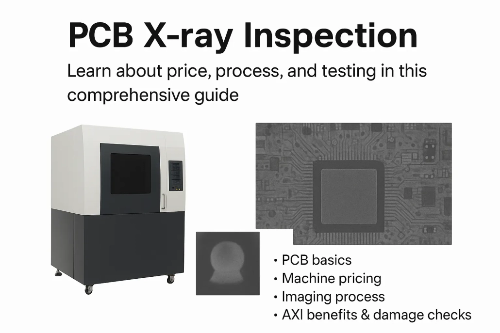
In modern electronics manufacturing, PCBs have become denser, more complex, and packed with components that are nearly impossible to inspect visually. Traditional optical inspection methods can reveal surface defects, but they fall short when it comes to hidden solder joints, multilayer structures, or internal cracks. This is where PCB X-ray inspection steps in—offering an unparalleled look inside the board without physically damaging it.
From automated X-ray inspection (AXI) systems in high-volume SMT lines to compact desktop units for prototyping labs, the technology has become essential for ensuring product reliability in industries like automotive, aerospace, consumer electronics, and medical devices.
What Does PCB Stand For and Why It Matters
PCB stands for Printed Circuit Board—the foundational platform on which all electronic components are mounted and interconnected. A single PCB can contain dozens of layers, intricate copper traces, and hundreds (or thousands) of solder joints. Even one defective hidden joint can cause intermittent failures or total product breakdown, which is why non-destructive internal inspection is a critical step in quality control.
Get a Quotation For PCB X-ray Now
What is PCB X-ray Inspection?
PCB X-ray inspection uses high-energy X-ray beams to penetrate the board and create images of its internal structures. The process can reveal:
-
Solder joint quality — Particularly in hidden package types like BGA (Ball Grid Array), QFN (Quad Flat No-lead), and CSP (Chip Scale Package).
-
Voids inside solder balls or joints.
-
Internal cracks or broken vias in multilayer PCBs.
-
Component misalignment or missing parts.
-
Bridging and short circuits not visible from the surface.
Types of PCB X-ray Inspection
-
2D X-ray — Quick, flat images ideal for basic defect detection.
-
3D X-ray (Computed Tomography / CT) — Cross-sectional imaging for precise failure analysis.
-
Laminography — Optimized for flat, layered structures like PCBs; combines speed with depth detail.
Get a Quotation For PCB X-ray Now
Automated X-ray Inspection (AXI)
In high-volume production, Automated X-ray Inspection integrates into the SMT line. Instead of manually loading and scanning boards, AXI systems automatically position, image, and analyze PCBs at production speeds.
Advantages of AXI:
-
Consistent defect detection without human bias.
-
Integration with MES (Manufacturing Execution Systems) for traceability.
-
High throughput—capable of inspecting hundreds of boards per hour.
-
Programmable defect criteria for specific components.
Get a Quotation For PCB X-ray Now
PCB X-ray Inspection Machine Price
The cost of a PCB X-ray inspection system varies widely depending on resolution, automation, and features.
| Machine Type | Typical Price Range | Example Models |
|---|---|---|
| Entry-level desktop (manual) | $20,000 – $50,000 | Manncorp MX1, basic Fischer models |
| Mid-range semi-automated | $60,000 – $150,000 | FISCHERSCOPE X-RAY XDLM, Nikon 2D systems |
| High-end 3D CT & laminography | $200,000+ | Nikon XT V 160, advanced inline AXI |
Cost Factors:
-
Resolution & Magnification — Measured in microns; higher resolution increases price.
-
Automation Level — Manual vs. fully automated.
-
Inspection Speed — Faster systems cost more.
-
Software Features — Auto defect recognition, AI analysis.
Get a Quotation For PCB X-ray Now
The Imaging Process of a PCB
A typical PCB X-ray imaging process involves:
-
Loading the PCB into the X-ray chamber or conveyor.
-
Setting beam parameters — Adjusting voltage (kV) and current (µA) to achieve proper penetration without overexposure.
-
Capturing Images — Using flat-panel detectors or image intensifiers.
-
Analyzing Data — The software flags voids, cracks, and misalignments.
-
Reporting — Results are logged and linked to PCB serial numbers for traceability.
For example, during BGA inspection, the X-ray clearly shows individual solder balls beneath the chip package, allowing engineers to spot voids or cold joints instantly.
Get a Quotation For PCB X-ray Now
PCB Test vs. PCB X-ray
While PCB functional testing checks electrical performance by powering the board and measuring signals, X-ray inspection focuses on structural integrity.
-
Functional Test — Detects whether the board works, but not why it fails.
-
X-ray Inspection — Reveals hidden physical defects that may not yet cause failure but could in the future.
Using both methods together ensures maximum product reliability.
Get a Quotation For PCB X-ray Now
How to Check if a PCB is Damaged
Damage detection can be divided into visible and hidden faults:
-
Visible Checks — Burn marks, cracked components, broken traces.
-
Electrical Testing — Using a multimeter or oscilloscope to find open/short circuits.
-
X-ray Inspection — For detecting voids, delamination, and hidden fractures.
In high-reliability applications (e.g., medical devices), X-ray inspection is the gold standard for detecting latent defects.
Get a Quotation For PCB X-ray Now
PCB Scanner vs. PCB X-ray
The term PCB scanner often refers to optical 2D scanners used for documenting layouts or reverse engineering.
While useful for surface features, optical scanners cannot see:
-
Internal copper layers.
-
Buried vias.
-
Solder joints under components.
PCB X-ray surpasses scanners by visualizing both surface and hidden structures.
Get a Quotation For PCB X-ray Now
Applications Beyond PCBs
X-ray inspection is not limited to PCBs. It is also widely used for:
-
Electronic components — Verifying IC die attach, wire bonds, and lead frame integrity.
-
Semiconductor packaging — Checking TSVs (Through-Silicon Vias) and micro-bumps.
-
Battery cells — Ensuring no internal shorting or contamination.
Get a Quotation For PCB X-ray Now
Choosing the Right X-ray Inspection Machine
When selecting a PCB X-ray inspection system, consider:
-
Resolution — For BGA void analysis, 2–5 µm resolution is often required.
-
Stage Size — Larger stages allow inspection of bigger boards or entire panels.
-
Throughput — Inline AXI for mass production vs. benchtop for R&D.
-
Software — Look for AI-assisted defect detection and reporting tools.
-
Brand Reputation — Nikon, Fischer, and Manncorp are trusted in the industry.

