
PCB Manufacturing Process: Step-by-Step Guide
Printed Circuit Boards (PCBs) are the backbone of modern electronics, serving as the foundation for electrical connections between components. Understanding the PCB manufacturing process is essential for designers, engineers, and manufacturers who aim to ensure reliability, performance, and cost-effectiveness in electronic products.
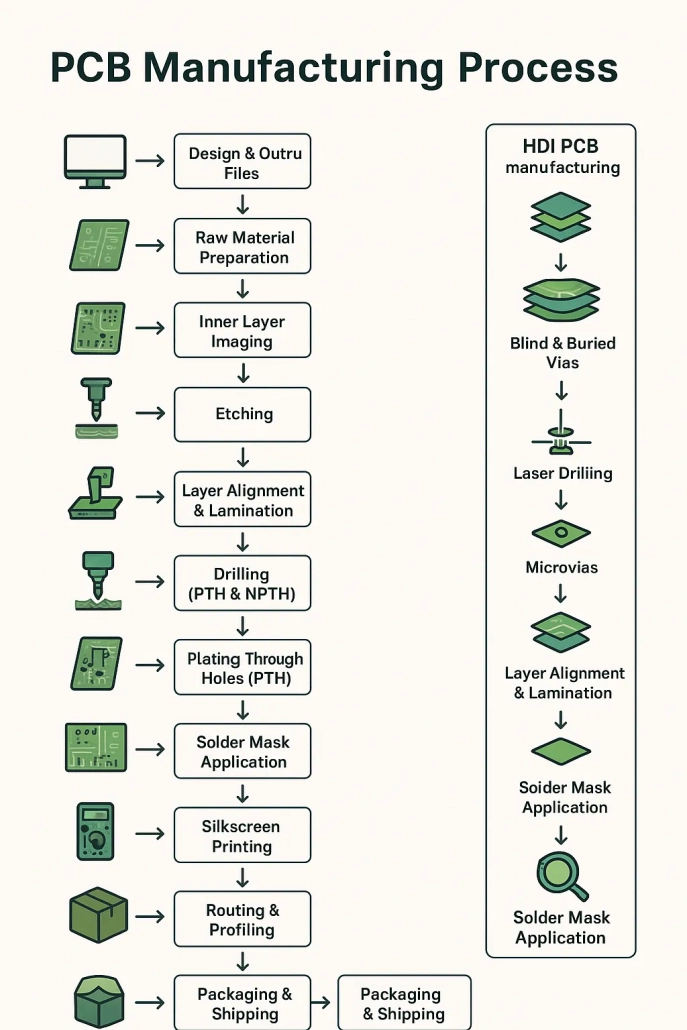
PCB Manufacturing Process Flow Overview
The PCB manufacturing process is a carefully controlled series of steps that turn raw materials into functional circuit boards. The flow may vary depending on whether it is a single-sided, double-sided, or multilayer PCB, but the overall structure is consistent.
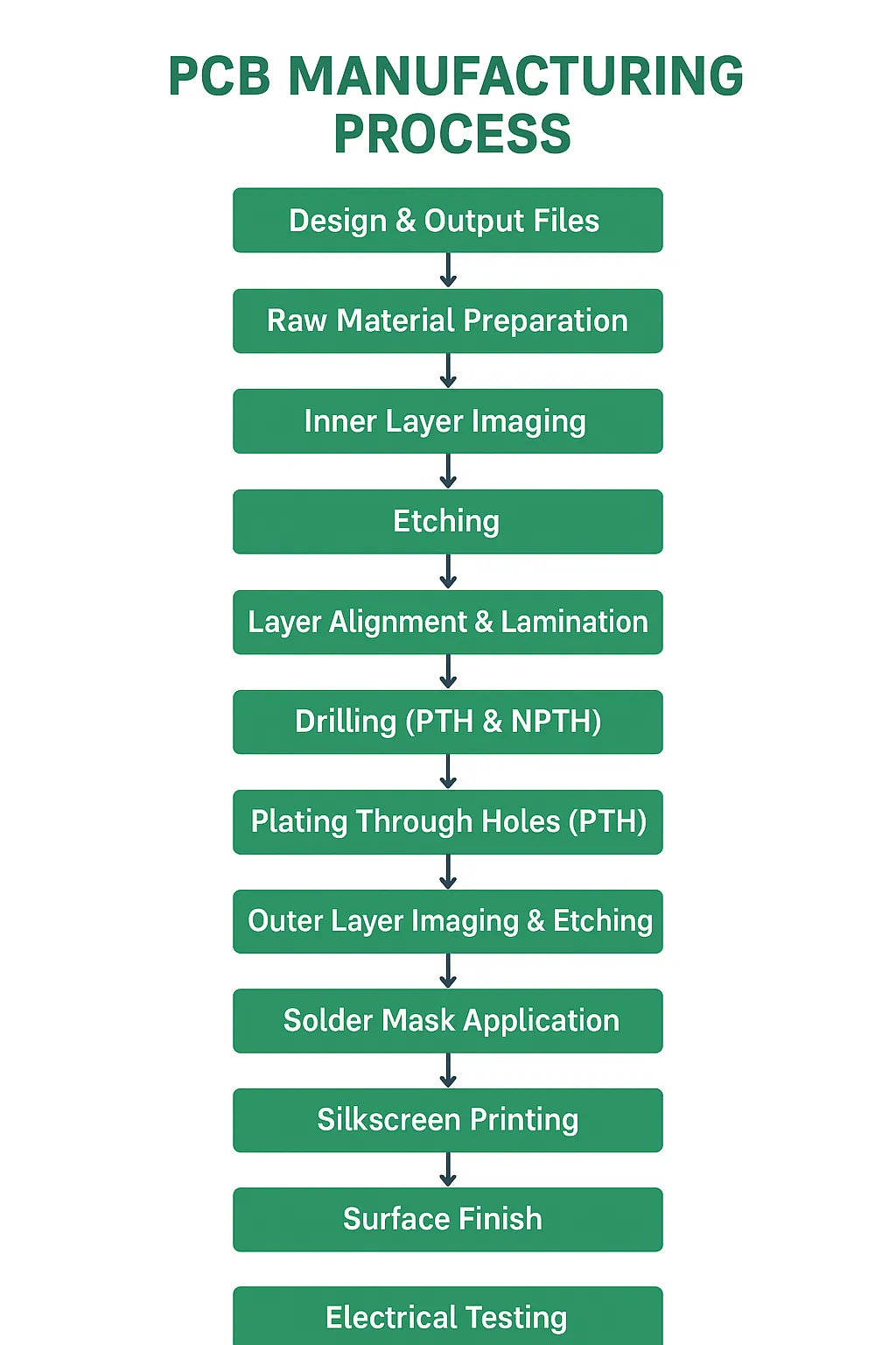
General PCB Manufacturing Process Flow:
- Design & Gerber File Output
- Raw Material Preparation
- Inner Layer Imaging & Etching
- Layer Alignment & Lamination
- Drilling (PTH & NPTH)
- Plating Through Holes (PTH)
- Outer Layer Imaging & Etching
- Solder Mask Application
- Silkscreen Printing
- Surface Finish
- Electrical Testing
- Profiling & Routing
- Final Inspection & Packaging
Get a Quotation For PCB Manufacturing Process Now
Step-by-Step PCB Manufacturing Process
1. Design & Output Files
Engineers design the PCB layout using CAD tools, generating Gerber files and drill data. The Bill of Materials (BOM) is also finalized.
2. Raw Material Preparation
Copper-clad laminates, prepregs, and insulating base materials such as FR4 or polyimide are cut to panel size for production.
3. Inner Layer Imaging
A layer of photoresist is applied to the copper surface. The PCB pattern is transferred via UV exposure, followed by chemical development.
4. Etching
Unwanted copper is chemically etched away, leaving only the designed circuit traces.
5. Lamination & Alignment
Multiple layers are stacked and laminated under heat and pressure. Optical alignment ensures precision across all layers.
6. Drilling (PTH & NPTH)
Holes for vias and components are drilled using CNC machines. Laser drilling is used for microvias in HDI PCBs.
7. Plating Through Holes (PTH)
Through-holes are plated with copper to form conductive interconnections between PCB layers.
8. Outer Layer Imaging & Etching
Outer copper layers are patterned and etched, defining the final circuit.
9. Solder Mask Application
A protective solder mask (green, blue, red, or black) is applied to insulate copper traces and prevent short circuits.
10. Silkscreen Printing
White silkscreen is applied to display component identifiers, logos, and reference markers.
11. Surface Finish
Surface finishes like HASL, ENIG, OSP, Immersion Silver, or Immersion Gold are applied for solderability and corrosion protection.
12. Electrical Testing
Flying probe or In-Circuit Testing (ICT) ensures that there are no open circuits or short circuits.
13. Profiling & Routing
PCBs are routed or punched into their final dimensions.
14. Final Inspection & Packaging
Automated Optical Inspection (AOI) and manual inspection confirm quality. Boards are packaged for shipment.
Get a Quotation For PCB Manufacturing Process Now
Special Processes in PCB Manufacturing
HDI PCB Manufacturing Process
High-Density Interconnect (HDI) PCBs require advanced steps such as:
- Sequential lamination
- Blind & buried vias
- Laser-drilled microvias
Flexible & Rigid-Flex PCBs
- Flexible PCBs use polyimide substrates for bendability.
- Rigid-flex designs combine flexibility with rigidity for compact, high-reliability applications.
Get a Quotation For PCB Manufacturing Process Now
PCB Manufacturing Machines & Automation
- CNC Drilling Machines – Create precise holes.
- Etching Lines – Remove unwanted copper.
- AOI Systems – Automated Optical Inspection for defect detection.
- X-ray Inspection – For hidden solder joints and multilayer analysis.
- Routing Machines – Cut PCBs into final shapes.
PCB Manufacturing in India
The PCB industry in India is growing rapidly due to government initiatives and increased demand for electronics. Local manufacturers are emerging as competitive players in the global supply chain, with India investing in both conventional PCB production and advanced HDI and flexible PCB technologies. Compared with China and Europe, India is still developing but has strong growth potential.
Get a Quotation For PCB Manufacturing Process Now
PCB Assembly: Raw Materials
Key raw materials in PCB manufacturing include:
- Base Laminates – FR4, Polyimide, CEM materials
- Copper Foil – Conductive layers
- Prepreg – Adhesive resin for lamination
- Solder Mask Inks – Protective coatings
- Surface Finish Chemicals – For HASL, ENIG, OSP, etc.
Get a Quotation For PCB Manufacturing Process Now
Common PCB Testing Methods
- Visual Inspection
- In-Circuit Test (ICT)
- Flying Probe Test
- Functional Test (FCT)
- Burn-in Test
- Automated Optical Inspection (AOI)
- X-ray Inspection (AXI)
Get a Quotation For PCB Manufacturing Process Now
DigiKey & PCB Manufacturing
A common question: Does DigiKey manufacture PCBs?
- DigiKey does not directly produce PCBs.
- Instead, it offers a PCB Builder Tool that connects engineers with manufacturing partners for prototype and small-batch orders.
Get a Quotation For PCB Manufacturing Process Now
PCB Manufacturing Resources
- PCB Manufacturing Process PDF – Downloadable technical reference materials.
- PCB Manufacturing Process PPT – Educational and training use.
- PCB Manufacturing Process Video – Factory walkthroughs and tutorials.
Conclusion
The PCB manufacturing process is a combination of precision engineering, advanced materials, and strict quality control. Each step, from Gerber design to final inspection, plays a critical role in ensuring reliability. With the rise of HDI, flexible PCBs, and automation, the industry continues to advance, powering the next generation of consumer electronics, automotive systems, and aerospace applications.

