
PCB Lamination Process & Sequential Lamination
Modern electronics rely on multilayer PCBs (Printed Circuit Boards) to achieve compact size, high performance, and complex interconnections. One of the most critical steps in building multilayer boards is PCB lamination—a process of bonding layers of copper foil and dielectric materials together under heat and pressure. While “lamination” in general refers to applying a protective layer on surfaces, PCB lamination is a far more advanced technique essential for electronic manufacturing.
What is PCB Lamination?
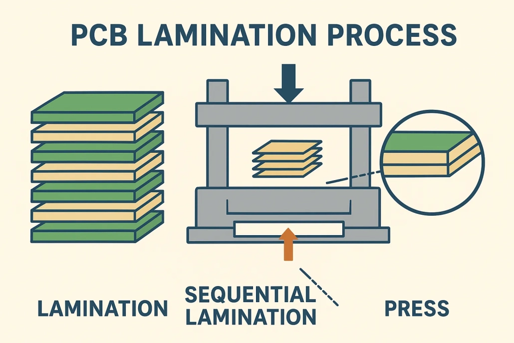
PCB lamination is the process of stacking multiple copper and dielectric layers, aligning them precisely, and pressing them together using heat, pressure, and time. During this process, prepreg (resin-impregnated fiberglass) melts and cures to bond copper foils with inner cores, forming a rigid and reliable multilayer board.
-
PCB Laminate vs PCB Lamination:
PCB Lamination Process Overview
The lamination cycle typically includes several carefully controlled stages:
-
Layer stackup preparation – core, prepreg, and copper foils are aligned.
-
Press loading – the stack is placed into a lamination press.
-
Heating and pressurizing – resin flows and fills gaps between copper layers.
-
Curing – resin hardens to create strong mechanical and electrical bonds.
-
Cooling and unloading – the laminated PCB panel is stabilized for further processing.
Typical Process Parameters
-
Temperature: 170°C – 230°C (depends on resin system).
-
Pressure: 150 – 300 psi (varies with board thickness and layer count).
-
Time: A full lamination cycle may take 1–2 hours including heating, pressing, and cooling.
Types of PCB Lamination
Standard Lamination
Used for conventional multilayer PCBs with moderate layer counts.
Sequential Lamination
For HDI (High-Density Interconnect) PCBs, sequential lamination builds layers step by step. This allows designers to create stacked vias, buried vias, and complex interconnects used in high-performance applications such as smartphones, servers, and AI processors.
Vacuum Lamination
An advanced method that eliminates air pockets (lamination voids), improving electrical reliability and thermal performance.
PCB Lamination Materials
The choice of materials significantly impacts performance.
-
Prepreg – resin-coated fiberglass sheets that bond copper foils and cores.
-
Core material – rigid dielectric base with copper foil already attached.
-
Common laminates:
-
FR4 (standard epoxy resin)
-
BT resin (substrates for IC packaging)
-
Polyimide (flexible and high-temperature resistant)
-
High-frequency laminates (Rogers, Panasonic, Taconic)
-
Advanced glass laminates (for next-gen HPC and AI packaging)
-
Major PCB Laminate Manufacturers
-
Isola Group
-
Rogers Corporation
-
Panasonic
-
Shengyi
-
Nan Ya Plastics
PCB Lamination Equipment
Modern PCB fabrication relies on PCB lamination presses:
-
Conventional hot presses – standard multilayer lamination.
-
Vacuum presses – reduce voids and improve quality.
-
Automated sequential lamination presses – used in high-volume HDI manufacturing.
Challenges & Defects in PCB Lamination
Even with advanced machinery, lamination faces common issues:
-
Lamination voids – air pockets causing signal loss and reliability issues.
-
Delamination – layers separating under stress or heat.
-
Misregistration – misaligned layers due to poor control.
-
Resin starvation – insufficient resin flow leading to weak bonding.
Manufacturers prevent these by controlling temperature profiles, applying vacuum lamination, and using advanced prepreg formulations.
PCB Lamination in the Overall Manufacturing Process
Lamination sits at the heart of the PCB manufacturing process. Once layers are laminated:
-
Drilling, via plating, imaging, and etching follow.
-
Proper lamination ensures electrical connectivity, thermal stability, and mechanical strength for subsequent steps.
Applications of Sequential Lamination
Sequential lamination is widely used in:
-
HDI PCBs – for smartphones, tablets, and networking equipment.
-
Semiconductor packaging substrates – FC-BGA, CSP, SiP substrates.
-
Automotive electronics – ADAS and EV power systems.
-
Aerospace & defense – high-reliability multilayer boards.
-
5G and AI systems – high-speed, low-loss interconnects.
Conclusion
PCB lamination is more than just pressing layers together—it defines the reliability, signal performance, and durability of modern PCBs. From basic multilayer designs to complex sequential lamination for HDI and packaging substrates, the process continues to evolve with new materials, vacuum technology, and advanced press systems. Looking forward, innovations such as glass laminates and eco-friendly resin systems will further push the boundaries of what PCB lamination can achieve.

