
Ensuring Reliability: Minimum Clearance in BGA PCBs
Printed Circuit Board (PCB) design and manufacturing are critical processes in the electronics industry, forming the backbone of almost all electronic devices. PCBs serve as the foundation for mounting and interconnecting various electronic components, from simple resistors to complex microprocessors. The design phase involves creating a layout that ensures optimal performance and reliability, while manufacturing transforms this layout into a physical board through precise fabrication techniques.
Understanding design rules and specifications is paramount for producing high-quality PCBs. These rules, such as trace width, spacing, and via size, dictate the electrical and physical properties of the board. Adhering to these specifications ensures signal integrity, minimizes electromagnetic interference (EMI), and enhances overall device performance. Moreover, compliance with manufacturing capabilities prevents defects, reduces production costs, and accelerates time-to-market. As the electronics industry advances, mastering these design principles is essential for innovation and maintaining competitive edge in the market.
Understanding PCB Design Rules
Explanation of the Critical Design Rules in PCB Manufacturing
Design rules in PCB manufacturing are essentially guidelines that engineers and designers must follow to ensure the functionality and reliability of printed circuit boards. These rules encompass a variety of parameters, including but not limited to trace width and spacing, via sizes, pad sizes, and clearance between different components. Each of these parameters plays a crucial role in determining how well a PCB will perform under various operational conditions.
Trace Width and Spacing: This rule dictates the width of the conductive paths and the distance between them, which affects the current carrying capacity and crosstalk between adjacent traces.
Via Size: Vias are small holes in a PCB that are filled or plated through to connect different layers. Their size impacts the reliability of these interconnections and the electrical performance of the PCB.
Pad Size: The size of the pads for mounting components must be sufficient to ensure a solid solder connection, while also considering solder mask dimensions to prevent solder bridging.
Clearance: The minimum distance between components and board edges, and between different conducting elements, which is critical for preventing short circuits and ensuring electrical safety.
Introduction to the 3W Rule and Its Significance
One of the less commonly discussed but crucially important design rules in PCB manufacturing is the “3W rule.” This rule states that the spacing between parallel traces should be at least three times the width of the widest trace involved. This rule is significant in managing EMI—Electromagnetic Interference—and signal integrity.
EMI Reduction: By increasing the distance between traces, the 3W rule helps in reducing the capacitive coupling between them, which in turn minimizes the chances of EMI. This is particularly important in high-speed or high-frequency PCBs where interference can significantly degrade performance.
Signal Integrity: Adequate spacing according to the 3W rule also prevents cross-talk between signals in adjacent traces, preserving the integrity of the data transmitted through the board. This is crucial in complex designs where multiple signals need to be transmitted simultaneously without interference.
The adherence to the 3W rule and other design rules ensures that the PCB will not only function as intended but also be durable and reliable throughout its operational lifespan. By understanding and implementing these critical design rules, designers can avoid common pitfalls that may lead to PCB failures, thereby enhancing the overall quality of the electronic devices they are designing.
JLCPCB’s Minimum Trace Clearance
Discussion on JLCPCB’s Capabilities and Standards for PCB Manufacturing
JLCPCB is one of the leading PCB manufacturing services known for its rapid prototyping and cost-effective production solutions. The company utilizes advanced manufacturing technologies and adheres to stringent quality control standards to ensure that each PCB meets the required specifications and performance criteria. JLCPCB offers a range of PCB capabilities including multi-layer boards, high-density interconnect (HDI) boards, and rigid or flexible PCB options. This versatility makes JLCPCB a preferred choice for a wide range of applications, from simple prototypes to complex, high-performance electronic assemblies.
Minimum Trace Clearance
One of the key specifications that JLCPCB enforces in its PCB manufacturing process is the minimum trace clearance. JLCPCB requires a minimum trace clearance of 0.15 mm (approximately 6 mils). This clearance is crucial for preventing electrical shorts and ensuring the physical separation of conductive paths, which is particularly important in densely packed boards where space optimization is critical. The specified clearance also helps in maintaining the integrity of electrical signals by reducing the risk of cross-talk and interference between adjacent traces.
Importance of Adhering to These Standards
Adhering to JLCPCB’s minimum trace clearance standard is essential for several reasons. Firstly, it significantly reduces the likelihood of manufacturing defects, which can lead to costly reworks or complete rejections of PCB batches. Ensuring the correct trace clearance during the design phase prevents issues such as unintentional bridging of traces during the etching or plating processes, which are common sources of short circuits in finished products.
Secondly, maintaining the specified clearance is crucial for the functionality and reliability of the PCB. In high-frequency or high-speed applications, even minor deviations from the set clearance can lead to significant degradation in performance due to increased electromagnetic interference and signal integrity issues. Moreover, following these standards ensures compatibility with the assembly processes, where components must be placed and soldered without the risk of electrical shorts.
In conclusion, adherence to JLCPCB’s standards like the minimum trace clearance is not merely about meeting production requirements; it is about ensuring that the final product performs as designed, with reliability over its intended lifespan. This adherence also streamlines the manufacturing process, enhancing overall efficiency and reducing turnaround times, which are critical factors in the fast-paced electronics industry.
BGA Footprint Design
Explanation of Ball Grid Array (BGA) Components
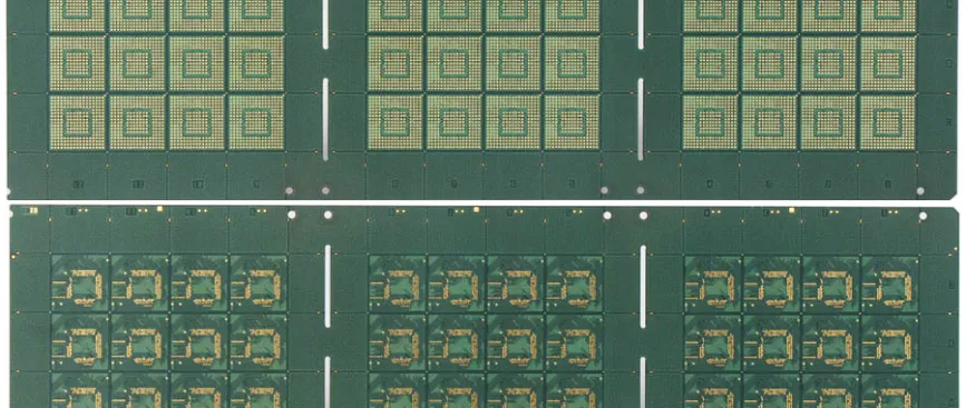
Ball Grid Array (BGA) components have become increasingly prevalent in modern PCB designs due to their numerous advantages over traditional packages. In a BGA, the connection points are located on the underside of the package in the form of small solder balls arranged in a grid pattern. This configuration offers several benefits, including reduced footprint, improved thermal performance, and better electrical performance at high frequencies. BGAs are commonly used in applications ranging from consumer electronics to aerospace and automotive industries, where compactness, reliability, and high pin count are essential.
Importance of Precise BGA Footprint Design
The BGA footprint design is critical to the overall performance and reliability of the PCB assembly. Since the solder balls are the primary means of electrical and mechanical connection between the BGA and the PCB, precise placement and alignment are crucial. A well-designed BGA footprint ensures proper soldering during assembly, minimizing the risk of solder defects such as solder bridges or insufficient solder joints. Moreover, a precise BGA footprint facilitates optimal thermal management, ensuring uniform heat dissipation across the component, which is essential for reliability, especially in high-power applications.
Key Considerations for Designing a BGA Footprint
When designing a BGA footprint, several key considerations must be taken into account to ensure optimal performance and reliability:
Pad Size: The size of the pads should be carefully chosen to provide sufficient surface area for solder attachment while maintaining adequate clearance between adjacent pads. Larger pads distribute mechanical stress more evenly, reducing the risk of pad lifting or solder joint fatigue.
Pitch: The pitch, or spacing between adjacent solder balls, determines the density of interconnections and affects the overall size of the BGA package. A finer pitch allows for higher pin counts in a smaller area but requires more precise manufacturing processes and may pose challenges during assembly.
Clearance: Adequate clearance between the solder balls and surrounding components or traces is essential to prevent short circuits and ensure electrical isolation. The clearance should be designed to accommodate variations in the manufacturing process, such as solder ball alignment tolerances and PCB surface flatness.
By carefully considering these factors and adhering to industry standards and best practices, designers can create BGA footprints that meet the requirements of their specific applications while ensuring reliable soldering and optimal electrical performance. Effective collaboration between PCB designers and manufacturers is essential to address any potential challenges and optimize the BGA footprint design for manufacturability and functionality.
Minimum Via Size for JLCPCB
Explanation of Vias and Their Role in Multi-layer PCBs
Vias are essential components in the construction of multi-layer PCBs, facilitating electrical connections between different layers of the board. They consist of plated-through holes that penetrate the entire thickness of the PCB, providing a conductive pathway for signals to travel vertically between layers. Vias play a crucial role in routing complex PCB designs by allowing designers to efficiently distribute signals and power across multiple layers while conserving valuable board space.
Minimum Via Size: JLCPCB’s Standards
JLCPCB maintains strict standards for via sizes to ensure the reliability and manufacturability of PCBs. The company’s standard minimum via size is 0.2 mm (approximately 8 mils) for the drill hole diameter, with a minimum annular ring of 0.15 mm (approximately 6 mils). This specification ensures that the vias are adequately sized to accommodate the required conductive plating while maintaining sufficient clearance between adjacent traces and other elements of the PCB layout.
Impact on Layout and Routing of PCB Designs
The minimum via size specified by JLCPCB has significant implications for the layout and routing of PCB designs. Designers must consider these specifications when planning the placement of components and routing of signal traces to ensure compliance with manufacturing requirements.
Routing Density: The minimum via size influences the routing density achievable within the available board space. Smaller vias allow for tighter packing of traces and components, enabling more efficient use of PCB real estate in densely populated designs.
Signal Integrity: Properly sized vias are crucial for maintaining signal integrity by minimizing impedance discontinuities and signal reflections. In high-speed digital or RF applications, where signal integrity is paramount, designers must carefully select via sizes to minimize signal degradation and ensure reliable performance.
Manufacturability: Adhering to JLCPCB’s minimum via size standards ensures manufacturability by preventing issues such as drill breakage or insufficient plating. Designers should avoid using vias that are smaller than the specified minimum size to mitigate the risk of manufacturing defects and ensure the integrity of the final product.
In summary, understanding the role of vias in multi-layer PCBs and adhering to JLCPCB’s minimum via size standards are essential for achieving reliable and manufacturable PCB designs. By considering these specifications during the design phase, designers can optimize layout and routing choices to meet the requirements of their specific applications while ensuring compatibility with JLCPCB’s manufacturing capabilities.
Designing for Minimum Clearance BGA PCB
Integrating Design Rules in PCB Design
Designing PCBs with Ball Grid Array (BGA) components requires careful integration of various design rules, including the 3W rule, minimum trace clearance, and via size requirements.
3W Rule Integration: Implementing the 3W rule ensures adequate spacing between traces to minimize interference and crosstalk. Designers should adjust trace widths and spacing to comply with this rule while optimizing signal integrity.
Minimum Trace Clearance and Via Size: Adhering to JLCPCB’s minimum trace clearance and via size standards is crucial for manufacturability. Designers should ensure that trace-to-trace and trace-to-via clearances meet the specified requirements to prevent manufacturing defects and ensure reliable operation.
Strategies for Optimizing BGA Footprints
Optimizing BGA footprints involves several strategies to maximize functionality and manufacturability while adhering to JLCPCB’s capabilities:
Pad Placement: Carefully position pads within the BGA footprint to maintain uniformity and minimize soldering issues. Ensure that the pad arrangement allows for proper alignment of solder balls during assembly.
Pad Size and Pitch: Select pad sizes and pitches that balance the requirements for solder joint reliability and space constraints. Larger pads provide more surface area for solder attachment, while finer pitches allow for higher pin counts but require precise manufacturing processes.
Thermal Considerations: Incorporate thermal vias or thermal relief pads into the BGA footprint design to improve heat dissipation and prevent overheating of the component. Proper thermal management is critical for maintaining reliability, especially in high-power applications.
Examples and Best Practices
To ensure reliable and efficient PCB designs with minimum clearance BGAs, designers can follow these examples and best practices:
Use Design Software Tools: Utilize PCB design software tools to implement design rules and verify compliance with manufacturing requirements. These tools offer features such as design rule checks (DRC) and layout optimization to streamline the design process.
Design Iteration and Validation: Perform iterative design iterations and validation to fine-tune BGA footprints and optimize performance. Conduct thorough simulations and prototype testing to verify functionality and reliability before mass production.
Collaborate with Manufacturers: Engage in collaborative discussions with PCB manufacturers like JLCPCB to address any design challenges and ensure alignment with manufacturing capabilities. Manufacturers can provide valuable insights and recommendations for optimizing BGA footprints and improving manufacturability.
By integrating design rules, implementing optimization strategies, and leveraging best practices, designers can create reliable and efficient PCB designs with minimum clearance BGAs that meet the requirements of their specific applications while ensuring compatibility with JLCPCB’s manufacturing capabilities.
FAQs about Minimum Clearance BGA PCB Manufacturer
The 3W rule in PCB refers to a design guideline that specifies the minimum distance between parallel traces. It states that the distance between traces should be at least three times the width of the widest trace involved. This rule helps in reducing interference and crosstalk between traces on the PCB.
The minimum trace clearance for JLCPCB is 0.15 mm (6 mils). This clearance refers to the minimum distance between adjacent traces on the PCB to prevent electrical shorts and ensure reliable functionality.
The BGA footprint refers to the arrangement and layout of pads on a printed circuit board (PCB) for a Ball Grid Array (BGA) component. BGAs are electronic packages with solder balls arranged in a grid pattern on the underside of the component. The footprint defines the positions, sizes, and spacing of the pads to facilitate soldering and electrical connections between the BGA and the PCB.
The minimum via size for JLCPCB is 0.2 mm (8 mils) for the drill hole diameter, with a minimum annular ring of 0.15 mm (6 mils). Vias are plated-through holes on the PCB used for interconnecting different layers or conducting signals to different parts of the board. JLCPCB specifies these minimum sizes to ensure reliable manufacturing and electrical performance of PCBs.

