
Compact and Reliable: The Rise of Leadless Chip Carrier
Semiconductor packaging technologies serve as the crucial interface between integrated circuits and their application environments. These technologies encompass various methods like Flip chip, Interposer, Dual in-line package (DIP), and more, each tailored to specific needs. Among these, Leadless Chip Carrier (LCC) emerges as a notable solution characterized by its compact design and versatile applications. LCC facilitates the secure mounting and interconnection of semiconductor chips onto circuit boards, offering a balance of performance, size, and cost-effectiveness. This introduction sets the stage to delve deeper into the realm of LCC packaging and its significance in modern electronics.
Understanding Semiconductor Packaging
Explanation of Different Packaging Technologies
Semiconductor packaging technologies encompass a diverse range of methods tailored to meet various requirements. These include:
1. Flip Chip: In this method, the semiconductor die is flipped upside down and directly mounted onto the substrate or carrier, allowing for shorter interconnect lengths and improved thermal performance.
2. Interposer: An interposer is a substrate that acts as an intermediary between the semiconductor die and the package substrate, enabling high-density interconnections and heterogeneous integration.
3. Dual in-line package (DIP): DIP is one of the earliest packaging formats, characterized by two parallel rows of connecting pins along the package’s periphery.
4. Chiplet: Chiplet packaging involves assembling multiple smaller semiconductor chips, or chiplets, onto a common substrate to create a larger functional system, enabling modular design and enhanced scalability.
5. Multi Chip Module (MCM): MCM integrates multiple semiconductor chips within a single package, often interconnected using advanced techniques like wire bonding or flip chip assembly.
Importance of Packaging in Semiconductor Industry
Semiconductor packaging plays a critical role in ensuring the reliability, performance, and functionality of integrated circuits. It provides protection from external environmental factors such as moisture, dust, and mechanical stress, while also facilitating electrical connections between the semiconductor die and the external circuitry.
Furthermore, packaging influences key metrics such as signal integrity, thermal management, and form factor, thereby directly impacting the overall performance and cost-effectiveness of electronic systems.
Transition Towards Advanced Packaging Solutions
The semiconductor industry is witnessing a significant transition towards advanced packaging solutions driven by the need for higher performance, increased functionality, and miniaturization. These advanced packaging technologies, such as 3D integration, fan-out wafer-level packaging (FOWLP), and system-in-package (SiP), offer enhanced electrical performance, reduced form factors, and improved integration capabilities compared to traditional packaging methods.
This transition underscores the industry’s ongoing efforts to address the evolving demands of emerging applications such as artificial intelligence, 5G telecommunications, and Internet of Things (IoT), where compactness, power efficiency, and performance are paramount.
Exploring PLCC and LCC
Definition and Characteristics
1. PLCC (Plastic Leaded Chip Carrier): PLCC is a type of semiconductor package that features a square or rectangular plastic body with leads (metal pins) extending from its four sides. The leads are typically arranged in a gull-wing or J-lead configuration, providing mechanical support and electrical connections between the integrated circuit (IC) chip and the external circuitry.
2. LCC (Leadless Chip Carrier): LCC is a semiconductor package that lacks external leads protruding from its body. Instead, it utilizes metal pads or balls on its underside for electrical connections. LCC packages come in various shapes and sizes, including square, rectangular, and custom configurations, offering flexibility in design and integration.
Key Differences Between PLCC and LCC Packaging
1. Lead Configuration: The most apparent difference between PLCC and LCC packaging lies in their lead configuration. PLCC packages feature external leads (pins), while LCC packages do not have external leads, relying instead on metal pads or balls for connectivity.
2. Mounting Method: PLCC packages are typically surface-mounted onto the circuit board, with the leads soldered onto corresponding pads. In contrast, LCC packages utilize surface mount technology (SMT) or ball grid array (BGA) techniques for attachment, where solder paste or solder balls create the electrical connections.
3. Size and Form Factor: LCC packages often offer a smaller footprint and lower profile compared to PLCC packages due to the absence of external leads. This compact form factor makes LCCs suitable for applications where space constraints are critical.
4. Thermal Performance: LCC packaging tends to exhibit better thermal performance compared to PLCC, as the absence of external leads allows for more efficient heat dissipation from the semiconductor die to the surrounding environment.
5. Cost: While PLCC packages may be more cost-effective in terms of manufacturing and assembly due to their simpler design and assembly process, LCC packages offer advantages in terms of size, performance, and thermal management, potentially justifying higher costs for certain applications.
Understanding these key differences between PLCC and LCC packaging is essential for selecting the most appropriate packaging solution based on the specific requirements of the semiconductor device and its intended application.
What is a PLCC Package?
Detailed Description of PLCC Packaging
PLCC (Plastic Leaded Chip Carrier) packaging is a popular type of semiconductor package known for its robustness, reliability, and versatility. The package consists of a square or rectangular plastic body, typically made from materials like epoxy or thermosetting plastics, providing mechanical support and protection for the enclosed semiconductor chip.
Components and Structure of PLCC
1. Plastic Body: The main body of the PLCC package houses the semiconductor chip and provides structural support. It is designed to withstand environmental stresses such as temperature fluctuations, mechanical shocks, and moisture.
2. Leads: PLCC packages feature leads (metal pins) extending from the sides of the plastic body. These leads are arranged in a gull-wing or J-lead configuration, facilitating easy mounting and soldering onto the surface of the circuit board.
3. Seal Ring: Some PLCC packages may include a seal ring around the perimeter of the package body to enhance moisture resistance and prevent the ingress of contaminants.
4. Integrated Circuit (IC) Chip: The semiconductor chip, also known as the die, is mounted within the PLCC package and connected to the leads via wire bonding or flip chip technology.
Applications and Use Cases of PLCC in Various Industries
PLCC packaging finds widespread use across various industries and applications, including:
– Consumer Electronics: PLCC packages are commonly found in consumer electronic devices such as televisions, smartphones, gaming consoles, and digital cameras, where they serve as the housing for integrated circuits like microcontrollers, memory chips, and signal processors.
– Automotive: In the automotive industry, PLCC packages are used in electronic control units (ECUs), sensors, and actuators for functions such as engine management, safety systems, and infotainment.
– Industrial Automation: PLCC packages are utilized in industrial automation systems for tasks such as process control, robotics, and monitoring, where reliability and durability are essential in harsh operating environments.
– Telecommunications: PLCC packages play a vital role in telecommunications infrastructure, including networking equipment, base stations, and optical transceivers, where they enable high-speed data processing and communication.
– Medical Devices: PLCC packaging is employed in medical devices and equipment for applications such as patient monitoring, diagnostic imaging, and therapeutic interventions, ensuring reliable performance and patient safety.
Overall, PLCC packaging offers a versatile and reliable solution for housing semiconductor chips in a wide range of electronic devices and systems, contributing to their functionality, performance, and longevity.
Functions of PLCC
Overview of the Role PLCC Plays in Semiconductor Devices
PLCC (Plastic Leaded Chip Carrier) packaging serves multiple crucial functions in semiconductor devices, contributing to their functionality, reliability, and longevity. Some of the key roles include:
1. Physical Protection: One of the primary functions of PLCC packaging is to provide physical protection to the enclosed semiconductor chip. The robust plastic body shields the delicate semiconductor die from environmental factors such as moisture, dust, mechanical shocks, and electrostatic discharge (ESD), ensuring its integrity and longevity.
2. Electrical Interconnection: PLCC packages facilitate the electrical interconnection between the semiconductor chip and the external circuitry. The metal leads extending from the package body serve as conductive pathways for transmitting signals and power between the integrated circuit (IC) chip and the rest of the electronic system.
3. Thermal Management: PLCC packaging plays a crucial role in dissipating heat generated by the semiconductor chip during operation. The package’s design and materials help to conduct heat away from the chip and distribute it to the surrounding environment, preventing overheating and maintaining optimal operating temperatures.
4. Mounting and Assembly: PLCC packages are designed for easy mounting and assembly onto the surface of the circuit board. The standardized lead configurations and mechanical dimensions ensure compatibility with automated assembly processes, reducing production time and costs.
Discussion on How PLCC Facilitates Connectivity and Protection of Integrated Circuits
1. Connectivity: PLCC packaging facilitates connectivity by providing a reliable interface between the semiconductor chip and the external circuitry. The metal leads extending from the package body establish electrical connections with corresponding pads on the circuit board through soldering or other attachment methods, ensuring secure transmission of signals and power.
2. Protection: PLCC packages offer robust protection to the enclosed semiconductor chip against various environmental hazards. The plastic body acts as a barrier, shielding the chip from moisture, dust, mechanical impacts, and ESD events that could otherwise compromise its functionality and reliability. Additionally, some PLCC packages may incorporate seal rings or other features to enhance moisture resistance and prevent contamination.
Overall, PLCC packaging plays a critical role in semiconductor devices by facilitating connectivity, providing physical protection, and ensuring efficient thermal management, ultimately contributing to the performance, reliability, and longevity of electronic systems.
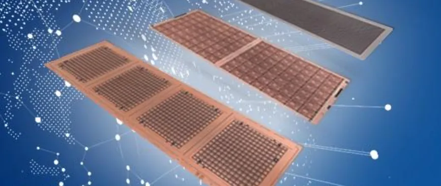
Understanding Leadless Chip Carrier (LCC)
Definition and Features of Leadless Chip Carrier
Leadless Chip Carrier (LCC) is a type of semiconductor packaging that differs from traditional packages like Plastic Leaded Chip Carrier (PLCC) in that it lacks external leads protruding from its body. Instead, LCC packages utilize metal pads or balls on their underside for electrical connections, allowing for a more compact and efficient design. Key features of LCC include:
1. Compact Form Factor: LCC packages are designed to be smaller and more space-efficient compared to traditional packaging solutions. The absence of external leads allows for a higher density of connections within a smaller footprint, making LCCs ideal for applications where size constraints are critical.
2. Enhanced Thermal Performance: The design of LCC packages often allows for better thermal dissipation compared to traditional packages. With the semiconductor chip directly mounted onto the substrate and the absence of leads, heat can be more efficiently transferred away from the chip, improving overall thermal management.
3. Improved Electrical Performance: LCC packages offer shorter electrical pathways and reduced parasitic capacitance and inductance compared to packages with longer lead lengths. This results in improved signal integrity, higher-speed operation, and better overall electrical performance in high-frequency applications.
Advantages of LCC over Traditional Packaging Solutions
1. Higher Integration Density: LCC packages enable higher integration density due to their compact form factor and the use of surface mount technology (SMT) or ball grid array (BGA) for electrical connections. This allows for more components to be packed into a smaller area, leading to more efficient use of board space and increased system functionality.
2. Improved Signal Integrity: The shorter electrical pathways in LCC packages reduce signal propagation delays and minimize signal degradation, resulting in improved signal integrity and reliability. This is particularly beneficial in high-speed digital and analog applications where signal fidelity is critical.
3. Enhanced Reliability: LCC packages typically exhibit improved reliability compared to traditional packages due to factors such as reduced mechanical stress on solder joints, better thermal management, and enhanced resistance to environmental hazards such as moisture and contamination.
4. Cost Efficiency: While LCC packages may have higher upfront manufacturing costs compared to traditional packages, their advantages in terms of size, performance, and reliability often justify the investment. Additionally, the higher integration density and improved system performance offered by LCCs can lead to overall cost savings in terms of reduced board space, simplified assembly processes, and enhanced product lifespan.
In summary, Leadless Chip Carrier (LCC) packaging offers numerous advantages over traditional packaging solutions, including a compact form factor, enhanced thermal and electrical performance, higher integration density, improved reliability, and cost efficiency. These features make LCCs well-suited for a wide range of applications in industries such as consumer electronics, telecommunications, automotive, and industrial automation.
Applications of Leadless Chip Carrier (LCC)
Industries and Applications Where LCC Packaging is Preferred
Leadless Chip Carrier (LCC) packaging finds widespread use across various industries and applications due to its compact form factor, enhanced performance, and reliability. Some industries and applications where LCC packaging is preferred include:
1. Consumer Electronics: LCC packages are commonly used in smartphones, tablets, laptops, and wearable devices for applications such as microprocessors, memory modules, and wireless communication chips. Their compact size and high integration density make them ideal for portable electronic devices where space constraints are critical.
2. Telecommunications: In the telecommunications industry, LCC packaging is employed in networking equipment, base stations, routers, and optical transceivers for high-speed data transmission, signal processing, and networking functions. LCCs offer improved signal integrity, thermal management, and reliability, making them well-suited for telecommunications infrastructure.
3. Automotive: LCC packages are increasingly being adopted in automotive electronics for applications such as engine control units (ECUs), advanced driver assistance systems (ADAS), infotainment systems, and vehicle-to-everything (V2X) communication modules. Their compact size, robustness, and resistance to temperature extremes make them suitable for use in harsh automotive environments.
4. Industrial Automation: LCC packaging is used in industrial automation systems, including programmable logic controllers (PLCs), motor drives, sensors, and actuators. Their high reliability, performance, and resistance to environmental hazards make them well-suited for applications in factories, warehouses, and industrial machinery.
Case Studies and Examples Showcasing the Versatility of LCC
1. Smartphones: LCC packages are extensively used in smartphones for components such as application processors, memory chips, and wireless connectivity modules. Their small size and high integration density enable manufacturers to pack powerful features into slim and lightweight devices while maintaining performance and reliability.
2. Data Centers: In data center equipment such as servers, switches, and storage devices, LCC packaging is preferred for high-speed processors, memory modules, and network interface cards. LCCs offer improved thermal management and signal integrity, allowing for efficient data processing and transmission in demanding server environments.
3. Medical Devices: LCC packages are utilized in medical devices and equipment such as patient monitors, diagnostic imaging systems, and surgical instruments. Their compact size, reliability, and resistance to environmental hazards make them suitable for use in medical applications where precision, performance, and safety are paramount.
4. Aerospace and Defense: LCC packaging is employed in aerospace and defense applications for components such as avionics systems, radar modules, communication systems, and guidance systems. Their high reliability, ruggedness, and resistance to temperature extremes make them well-suited for use in aircraft, satellites, missiles, and unmanned aerial vehicles (UAVs).
These case studies and examples highlight the versatility and wide-ranging applications of Leadless Chip Carrier (LCC) packaging across various industries, demonstrating its importance in enabling advanced electronic systems and technologies.
FAQs about leadless chip carrier
PLCC (Plastic Leaded Chip Carrier) has external leads (pins) protruding from its body, while LCC (Leadless Chip Carrier) lacks external leads and uses metal pads or balls on its underside for electrical connections.
A PLCC package is a type of semiconductor packaging that features a square or rectangular plastic body with leads (metal pins) extending from its sides. It provides mechanical support and electrical connections for semiconductor chips, facilitating their integration into electronic circuits.
PLCC packages serve several functions in semiconductor devices. They provide physical protection to enclosed semiconductor chips, establish electrical connections between the chip and external circuitry through leads, aid in thermal management by dissipating heat generated by the chip, and enable easy mounting and assembly onto circuit boards.
A chip carrier serves as a housing or package for semiconductor chips, providing mechanical support, electrical connections, and protection to the enclosed chip. It facilitates the integration of chips into electronic systems by enabling their connection to external circuitry and ensuring their reliable operation in various environmental conditions.

