
Unveiling Advanced IC Packaging Techniques
In the realm of semiconductor engineering, IC chip packaging refers to the process of enclosing integrated circuits (ICs) within protective casings. This crucial step ensures the safeguarding of delicate circuitry from external elements, mechanical stresses, and electromagnetic interference. Beyond mere protection, packaging plays a pivotal role in enhancing the performance, reliability, and functionality of semiconductor devices. It facilitates efficient heat dissipation, electrical connections, and signal propagation, thereby optimizing overall system performance. Additionally, IC packaging enables miniaturization, enabling the creation of compact electronic devices vital in modern technology. Consequently, understanding the intricacies of IC chip packaging is fundamental in advancing semiconductor technology and meeting the ever-evolving demands of diverse applications.
Common Types of IC Packaging
- Semiconductor Package:
- Semiconductor packages encapsulate the integrated circuit chips, providing physical protection and electrical connections. These packages come in various forms, ranging from simple designs to more complex configurations tailored for specific applications.
- SOP Package (Small Outline Package):
- SOP packages are characterized by their compact size and low profile, making them suitable for space-constrained applications like mobile devices and consumer electronics. They typically feature leads on two sides of the package, enhancing ease of PCB assembly.
- Chip Package:
- Chip packages, also known as die-level packages, involve directly bonding the bare semiconductor die onto a substrate or carrier. This minimalist approach reduces package size and enhances thermal performance, making it ideal for high-performance applications such as CPUs and GPUs.
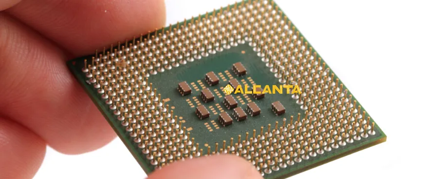
- LGA Package (Land Grid Array):
- LGA packages feature an array of solder pads on the underside of the package instead of leads, offering improved electrical and thermal properties. This design facilitates reliable connections and efficient heat dissipation, making LGAs suitable for high-power applications like microprocessors and power amplifiers.
- Dual In-line Package (DIP):
- DIP packages are among the earliest forms of IC packaging, featuring two parallel rows of pins along the package’s sides. While less common in modern electronics, DIPs are still utilized in certain applications, particularly in industries requiring through-hole mounting.
Comparison of Different Packaging Types
- Size: Compare the dimensions and form factors of each packaging type, highlighting their suitability for different applications based on space constraints.
- Electrical Performance: Discuss the electrical characteristics of each package, such as signal integrity, power delivery, and thermal management.
- Manufacturing Considerations: Explore the ease of manufacturing and assembly for each packaging type, including factors like cost, yield, and complexity.
- Application Specifics: Provide examples of industries or applications where each packaging type excels, showcasing their versatility and adaptability to diverse requirements.
- Trends and Evolution: Touch upon how these packaging types have evolved over time to meet the demands of advancing technology, including emerging trends in miniaturization, performance, and reliability.
Most Common IC Packaging
Among the various types of IC packaging, the SOP (Small Outline Package) stands out as one of the most prevalent and widely adopted forms. Its dominance in the semiconductor industry can be attributed to several key factors:
- Compact Size and Low Profile:
- SOP packages offer a compact footprint and low profile, making them ideal for applications where space is limited. This characteristic is particularly advantageous in the design of portable electronic devices such as smartphones, tablets, and wearables.
- Ease of Handling and Assembly:
- SOP packages feature leads on two sides of the package, facilitating automated assembly processes such as surface-mount technology (SMT). The standardized lead configuration simplifies PCB layout and manufacturing, reducing production costs and improving overall efficiency.
- Enhanced Thermal Performance:
- Despite their small size, SOP packages often incorporate innovative thermal management features, such as exposed thermal pads or heat sinks. These design elements help dissipate heat efficiently, ensuring reliable operation even in demanding environments.
- Versatility and Compatibility:
- SOP packages are available in various configurations, including SOP8, SOP16, and SOP28, among others, catering to a wide range of semiconductor devices. Furthermore, their compatibility with standard IC sockets and connectors enhances versatility and ease of integration into existing systems.
- Industry Standardization and Adoption:
- Over the years, SOP packages have become standardized within the semiconductor industry, with manufacturers and designers alike favoring their proven reliability and performance. This widespread adoption has further solidified SOP’s position as the go-to choice for many electronic applications.
- Cost-Efficiency:
- SOP packages offer a cost-effective solution for packaging integrated circuits, balancing performance, and affordability. Their streamlined design and mass production capabilities contribute to lower manufacturing costs, making them an attractive option for high-volume production.
The prevalence of SOP packages in the semiconductor industry can be attributed to their compact size, ease of handling, thermal performance, versatility, industry standardization, and cost-efficiency. These factors collectively position SOP packages as the most common and preferred choice for a wide range of electronic devices and applications.
Materials Used for Chip Packaging
Chip packaging involves the encapsulation of integrated circuits (ICs) within protective casings, and the choice of materials plays a crucial role in determining the performance, reliability, and functionality of the packaged chips. Here’s an overview of materials commonly used in chip packaging, highlighting their properties and applications:
- Plastic:
- Plastic materials, such as epoxy resins and thermoplastics (e.g., polyethylene, polypropylene), are widely used in chip packaging due to their low cost, ease of manufacturing, and versatility.
- Properties:
- Thermal Conductivity: Generally lower compared to other materials, which may require additional thermal management solutions.
- Electrical Insulation: Excellent electrical insulation properties, preventing short circuits and electrical leakage.
- Mechanical Strength: Moderate mechanical strength, suitable for protecting chips from external stresses and impacts.
- Applications: Consumer electronics, automotive components, and low-power devices.
- Ceramic:
- Ceramic materials, including alumina (Al2O3) and aluminum nitride (AlN), are favored for their superior thermal conductivity and reliability, particularly in high-power and high-frequency applications.
- Properties:
- Thermal Conductivity: Excellent thermal conductivity, facilitating efficient heat dissipation and reducing operating temperatures.
- Electrical Insulation: High electrical insulation properties, crucial for preventing signal interference and breakdown.
- Mechanical Strength: High mechanical strength, providing robust protection against mechanical shocks and vibrations.
- Applications: Power modules, RF/microwave components, and high-temperature environments.
- Metal:
- Metal packaging, typically made of alloys like aluminum or copper, offers exceptional thermal conductivity and mechanical stability, making it suitable for demanding applications requiring efficient heat dissipation and rugged protection.
- Properties:
- Thermal Conductivity: High thermal conductivity, enabling rapid heat transfer and dissipation.
- Electrical Insulation: Requires additional insulating layers to prevent electrical shorts in some configurations.
- Mechanical Strength: Excellent mechanical strength, providing durability and protection against environmental stresses.
- Applications: Power semiconductor devices, high-power LEDs, and military/aerospace electronics.
- Composite Materials:
- Composite materials, combining properties of different materials (e.g., plastics reinforced with glass fibers), offer a balance of thermal performance, electrical insulation, and mechanical strength, tailored to specific application requirements.
- Properties:
- Thermal Conductivity: Varies depending on the composition, often intermediate between pure plastics and ceramics/metals.
- Electrical Insulation: Can be engineered to provide adequate electrical insulation while maintaining other desired properties.
- Mechanical Strength: Enhanced mechanical strength compared to pure plastics, suitable for applications requiring improved ruggedness.
- Applications: Aerospace, automotive powertrain modules, and industrial sensors.
In summary, the choice of packaging materials in chip packaging is driven by the specific requirements of the application, balancing factors such as thermal conductivity, electrical insulation, and mechanical strength to ensure optimal performance and reliability of the packaged ICs.
Advanced IC Packaging
As technology continues to evolve, so does the field of IC packaging. Advanced packaging techniques have emerged to address the ever-increasing demand for smaller, faster, and more energy-efficient semiconductor devices. Here’s an in-depth look at advanced IC packaging:
1. Definition and Significance of Advanced Packaging
- Advanced packaging refers to innovative techniques that go beyond traditional methods to achieve higher levels of integration, performance, and functionality in semiconductor devices.
- Significance:
- Enables higher levels of miniaturization, allowing for the development of smaller and more powerful electronic products.
- Enhances system-level performance by improving thermal management, signal integrity, and power efficiency.
- Facilitates heterogeneous integration, enabling the integration of different semiconductor technologies on a single chip or package.
2. Emerging Trends and Technologies in Advanced Packaging
- 3D Packaging: Involves stacking multiple dies vertically to increase packaging density and reduce interconnect lengths, enhancing performance and reducing footprint.
- System-in-Package (SiP): Integrates multiple functional components, such as processors, memory, and sensors, into a single package, improving overall system performance and reducing system-level complexity.
- Embedded Die Packaging: Embeds semiconductor dies within substrate materials, enabling higher levels of integration and improved thermal performance.
- Through-Silicon Via (TSV) Technology: Facilitates vertical interconnects through the silicon substrate, enabling faster data transfer rates and reduced power consumption.
- Advanced Interconnect Technologies: Includes technologies such as microbumps, redistribution layers (RDL), and fine-pitch bonding, enabling high-density interconnects and improved signal integrity.
3. Fan-Out Wafer Level Packaging (FOWLP)
- FOWLP is an advanced packaging technology that involves redistributing the active components of a semiconductor device from the chip’s surface to the wafer level, allowing for greater flexibility in package design and improved electrical performance.
- Benefits:
- Reduced form factor and footprint, enabling thinner and lighter devices.
- Improved thermal performance and reliability due to shorter interconnect lengths.
- Enhanced signal integrity and electrical performance.
- Challenges:
- Complexity of manufacturing processes and equipment.
- Higher cost compared to traditional packaging methods.
- Limited availability of design and manufacturing expertise.
4. Wafer Level Packaging (WLP)
- WLP involves packaging semiconductor devices at the wafer level, eliminating the need for individual packaging of each die and reducing overall packaging costs.
- Benefits:
- Improved manufacturing efficiency and yield.
- Enhanced thermal management and electrical performance.
- Enables the integration of MEMS (Micro-Electro-Mechanical Systems) and RF (Radio Frequency) components.
- Challenges:
- Limited scalability for large die sizes.
- Higher upfront investment in infrastructure and equipment.
- Potential reliability issues related to handling and testing at the wafer level.
In conclusion, advanced IC packaging techniques play a crucial role in driving innovation and meeting the demands of modern electronic devices. While these technologies offer numerous benefits, they also present challenges that require careful consideration and expertise to overcome. As the semiconductor industry continues to push the boundaries of what’s possible, advanced packaging will remain a key enabler of progress and innovation.
IC Packaging and Testing
In the semiconductor industry, IC packaging and testing are interdependent processes crucial for ensuring the reliability, functionality, and performance of integrated circuits. Here’s a detailed exploration of their relationship, the importance of testing, and an overview of testing methods and equipment:
1. Relationship between Packaging and Testing Processes
- Packaging and testing are integral parts of the semiconductor manufacturing flow, closely linked to ensure the quality and reliability of ICs.
- Packaging encapsulates the integrated circuit within a protective casing, while testing verifies the functionality and performance of the packaged IC.
- Packaging affects the accessibility of the die and the reliability of electrical connections, which directly impact the testing process.
- Testing identifies defects introduced during packaging, such as shorts, opens, and faulty connections, allowing for corrective measures to be taken before the ICs are shipped to customers.
2. Importance of Testing in Ensuring Reliability and Functionality
- Testing is critical for identifying manufacturing defects, ensuring that only functional ICs are delivered to customers.
- It helps verify the functionality of individual components and the integrity of interconnects, ensuring that the IC meets its specifications.
- Testing also evaluates the IC’s performance under various operating conditions, such as temperature and voltage, to ensure reliability and longevity.
- By detecting defects early in the manufacturing process, testing reduces the likelihood of field failures and warranty claims, thereby enhancing customer satisfaction and brand reputation.
3. Overview of Testing Methods and Equipment Used in IC Packaging
- Electrical Testing: Involves applying electrical stimuli to the IC and measuring its responses to verify functionality and performance. This includes tests such as continuity, functional, parametric, and speed testing.
- Burn-In Testing: Subjects the IC to prolonged periods of operation under elevated temperatures and voltages to detect and eliminate potential reliability issues caused by infant mortality or latent defects.
- Reliability Testing: Evaluates the IC’s long-term reliability by subjecting it to accelerated aging tests, thermal cycling, humidity testing, and other stress tests to simulate real-world operating conditions.
- Automated Test Equipment (ATE): Specialized testing equipment designed to automate the testing process, including semiconductor test systems, probe stations, handlers, and test sockets.
- In-Circuit Testing (ICT): Tests the IC while it is mounted on the PCB, verifying its functionality within the context of the entire system.
- Boundary Scan Testing: Utilizes standardized interfaces (e.g., JTAG) to access and test the interconnects and functionality of digital ICs, especially useful for complex PCBs with high pin counts.
IC packaging and testing are indispensable processes in semiconductor manufacturing, working hand in hand to ensure the reliability, functionality, and performance of integrated circuits. Through rigorous testing, defects are identified and corrected, ultimately contributing to the production of high-quality ICs that meet the stringent demands of modern electronic applications.
Future Trends in IC Packaging
The future of IC packaging is poised for exciting advancements driven by technological innovation and evolving market demands. Here’s a detailed exploration of predicted trends, potential advancements, and the impact of emerging technologies:
1. Predictions for the Future of IC Packaging
- Miniaturization: Continued miniaturization of electronic devices will drive demand for smaller, more compact packaging solutions, such as advanced 3D packaging technologies and embedded die packaging.
- Heterogeneous Integration: Increasing integration of diverse semiconductor technologies (e.g., logic, memory, sensors) on a single chip or package will necessitate advanced packaging techniques capable of accommodating different materials, processes, and functionalities.
- Enhanced Performance: Future IC packaging solutions will focus on improving electrical performance, thermal management, and signal integrity to meet the requirements of high-speed computing, artificial intelligence, and 5G communications.
- Sustainability: There will be a growing emphasis on environmentally sustainable packaging materials and manufacturing processes to reduce waste, energy consumption, and carbon footprint throughout the semiconductor supply chain.
2. Potential Advancements in Materials, Design, and Manufacturing Processes
- Advanced Materials: Development of novel materials with superior thermal conductivity, electrical properties, and mechanical strength will enable more efficient and reliable IC packaging solutions. This includes the use of carbon nanotubes, graphene, and advanced polymers.
- Innovative Designs: Future IC packaging designs may incorporate advanced architectures, such as hierarchical or reconfigurable structures, to optimize performance, power efficiency, and manufacturing scalability.
- Additive Manufacturing: Adoption of additive manufacturing (3D printing) techniques for rapid prototyping and production of customized packaging solutions, offering greater design flexibility and cost-effectiveness.
- Advanced Manufacturing Processes: Integration of advanced manufacturing processes, such as laser ablation, nanoimprint lithography, and atomic layer deposition, to achieve higher precision, resolution, and throughput in IC packaging production.
3. Impact of Emerging Technologies like AI, IoT, and 5G on Packaging Requirements
- Artificial Intelligence (AI): AI-driven applications will require IC packaging solutions capable of handling massive data processing, high-speed computation, and efficient thermal management to support AI chips’ performance requirements.
- Internet of Things (IoT): The proliferation of IoT devices will drive demand for low-power, compact packaging solutions with integrated sensors, wireless connectivity, and enhanced reliability for diverse IoT applications.
- 5G Communications: The rollout of 5G networks will drive the need for IC packaging solutions capable of supporting higher data rates, lower latency, and increased bandwidth, necessitating advancements in RF packaging, antenna integration, and thermal dissipation.
The future of IC packaging will be characterized by continuous innovation in materials, design, and manufacturing processes to meet the evolving demands of miniaturization, heterogeneous integration, enhanced performance, and sustainability. The convergence of emerging technologies like AI, IoT, and 5G will further drive the development of advanced packaging solutions to enable the next generation of electronic devices and applications.
FAQs About IC chip packaging
IC packaging refers to the process of enclosing integrated circuits (ICs) within protective casings, which provide physical protection and electrical connections. This packaging is essential for safeguarding delicate circuitry from external elements, mechanical stresses, and electromagnetic interference, while also facilitating efficient heat dissipation and signal propagation.
The most common IC packaging is the Small Outline Package (SOP), characterized by its compact size, low profile, and leads on two sides of the package. SOP packages are widely used in various electronic devices, including smartphones, tablets, and consumer electronics, due to their versatility, ease of handling, and compatibility with surface-mount technology (SMT) assembly processes.
Various materials are used for chip packaging, depending on the specific requirements of the application. Common materials include plastics (e.g., epoxy resins, thermoplastics), ceramics (e.g., alumina, aluminum nitride), metals (e.g., aluminum, copper), and composite materials (e.g., plastics reinforced with glass fibers). Each material offers different properties such as thermal conductivity, electrical insulation, and mechanical strength, which are crucial for ensuring the reliability and performance of the packaged chips.
Advanced IC packaging refers to innovative packaging techniques that go beyond traditional methods to achieve higher levels of integration, performance, and functionality in semiconductor devices. These advanced packaging technologies include 3D packaging, System-in-Package (SiP), wafer-level packaging (WLP), fan-out wafer-level packaging (FOWLP), and heterogeneous integration. Advanced IC packaging aims to address the demands of emerging technologies such as artificial intelligence (AI), Internet of Things (IoT), and 5G communications by offering solutions that enhance miniaturization, improve thermal management, and optimize signal integrity.


发表评论
Want to join the discussion?Feel free to contribute!