
Mastering Precision: Soldering QFN Packages
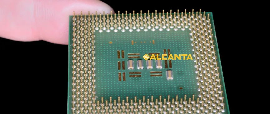
Quad Flat No-leads (QFN) packages are a popular choice in modern electronics due to their compact size, excellent thermal performance, and reliable electrical connections. These packages feature a flat bottom surface with exposed pads for soldering, eliminating the need for traditional leads.
Proper soldering techniques for QFN packages are crucial for ensuring optimal functionality and reliability of electronic devices. The intricate design of QFN packages demands precision during soldering to prevent issues such as poor connections, solder bridges, or misalignment, which can lead to performance degradation or even device failure. In this guide, we will delve into the essential methods and tools required to master the art of soldering QFN packages effectively.
Understanding QFN Soldering Challenges
Soldering QFN (Quad Flat No-leads) packages presents unique challenges due to their design, which lacks traditional leads and exposes the soldering pads underneath. Here are some common soldering problems encountered with QFN packages:
1. Solder Bridging: The close proximity of solder pads in QFN packages increases the risk of solder bridging, where solder unintentionally connects adjacent pads. This can short-circuit connections and lead to malfunctioning circuits.
2. Insufficient Solder Joint Formation: Achieving proper solder joint formation can be tricky with QFN packages, especially due to the small size of the pads. Inadequate solder coverage or incomplete wetting can result in weak connections, affecting electrical conductivity and reliability.
3. Misalignment: Misalignment of the QFN package during soldering can lead to skewed solder joints, causing poor contact with the PCB and compromising signal integrity.
4. Void Formation: Excessive voids within solder joints can occur due to factors like improper solder paste application or inadequate temperature control during reflow, potentially impacting thermal dissipation and electrical performance.
Addressing these challenges is paramount for ensuring reliable circuitry:
– Electrical Performance: Proper soldering techniques directly impact the electrical performance of QFN packages, including signal integrity, power distribution, and thermal management. Addressing soldering challenges helps maintain consistent electrical properties across the circuit.
– Mechanical Stability: Solder joints that are prone to defects such as bridging or insufficient bonding jeopardize the mechanical stability of the assembly. By overcoming soldering challenges, the mechanical integrity of the QFN package on the PCB is ensured, reducing the risk of physical damage or disconnection.
– Product Reliability: Reliable soldering techniques enhance the overall reliability of electronic products. By mitigating soldering challenges, the likelihood of premature failures or malfunctions due to solder-related issues is minimized, leading to increased product lifespan and customer satisfaction.
In the subsequent sections of this guide, we will explore in-depth the tools, techniques, and best practices for soldering QFN packages effectively, addressing these challenges to achieve optimal circuit performance and reliability.
Tools and Materials Required
1. Hot Air Rework Station:
– Features: A hot air rework station is essential for reflow soldering of QFN packages. Look for stations with adjustable temperature and airflow settings to cater to different QFN package sizes and board requirements. Digital displays and precise temperature control ensure accuracy during soldering.
– Functionalities: Hot air rework stations provide a consistent stream of hot air to melt solder paste, facilitating the reflow process. They allow targeted heating of specific areas, minimizing the risk of overheating sensitive components adjacent to the QFN package.
2. Soldering Iron:
– Types: When hand soldering QFN packages, choose soldering irons with fine tips and adjustable temperature settings. Temperature-controlled soldering irons ensure precise heat application, preventing overheating and damage to the QFN package or surrounding components. Thin, pencil-shaped irons offer better maneuverability and access to tight spaces on the PCB.
3. Flux:
– Importance: Flux is crucial for successful soldering of QFN packages as it promotes solder wetting, prevents oxidation of metal surfaces, and improves solder flow. Select a flux specifically formulated for surface mount components to ensure compatibility with the QFN package and PCB materials.
– Types: There are various types of flux available, including liquid flux, paste flux, and flux pens. Choose a flux type based on your soldering method and preference. Paste flux is often preferred for QFN soldering due to its controlled application and ability to stay in place during reflow.
4. Solder Paste:
– Choosing the Right Type: Selecting the correct solder paste is crucial for achieving reliable solder joints on QFN packages. Opt for solder pastes with a fine particle size and appropriate flux content. Lead-free solder pastes are commonly used to comply with environmental regulations. Ensure the solder paste’s melting temperature matches the reflow profile recommended for the QFN package.
5. Tweezers and Magnifying Glass:
– Enhancing Precision: Tweezers are indispensable for handling small components like QFN packages during soldering. Choose tweezers with fine tips and ergonomic handles for comfortable and precise manipulation. A magnifying glass or magnifying lamp aids in inspecting solder joints and verifying alignment, especially when working with intricate QFN packages and densely populated PCBs.
Equipping yourself with the right tools and materials is essential for achieving successful soldering of QFN packages. Each component plays a critical role in ensuring precise soldering, reliable electrical connections, and overall quality of the finished assembly.
Preparing for Soldering
1. PCB Preparation: Cleaning and Inspection
– Cleaning: Before soldering QFN packages, it’s essential to thoroughly clean the PCB surface to remove any contaminants such as dust, grease, or residues. Use a mild cleaning solution and a lint-free cloth or brush to gently scrub the PCB surface. Ensure the PCB is completely dry before proceeding with soldering.
– Inspection: After cleaning, inspect the PCB for any visible defects or damage, such as scratches, solder mask irregularities, or lifted pads. Address any issues found during the inspection to prevent soldering complications and ensure the integrity of the solder joints.
2. Component Preparation: Proper Handling and Alignment
– Handling: Handle QFN packages with care to prevent damage to the delicate leads or exposed pads. Use anti-static precautions to avoid electrostatic discharge (ESD) damage. When picking up QFN packages, hold them by the edges or use tweezers to minimize contact with the sensitive areas.
– Alignment: Proper alignment of the QFN package on the PCB is crucial for achieving accurate solder joints. Use alignment marks or reference points on the PCB to position the QFN package correctly. Ensure the orientation of the package matches the PCB footprint to prevent misalignment during soldering.
3. Flux Application: Techniques to Ensure Proper Coverage
– Selection: Choose a flux suitable for the soldering method (e.g., reflow or hand soldering) and compatible with the materials used in the QFN package and PCB. Apply a flux with a fine-tipped applicator or flux pen for precise control and targeted coverage.
– Application: Apply flux to the exposed pads on the PCB using a thin, even layer. Ensure complete coverage of the soldering area while avoiding excessive flux that could cause solder bridging or flux residue buildup. Flux promotes solder wetting and improves the flow of solder during reflow or hand soldering, resulting in reliable solder joints.
– Cleaning: After soldering, thoroughly clean the PCB to remove any flux residue using a suitable cleaning solution and a soft brush. Flux residue left on the PCB surface can lead to corrosion or electrical issues over time if not properly removed.
Proper preparation before soldering QFN packages is critical for achieving successful solder joints and ensuring the overall reliability of the electronic assembly. By meticulously cleaning and inspecting the PCB, handling components with care, and applying flux accurately, you can minimize the risk of soldering defects and optimize the performance of the QFN package on the PCB.
Soldering QFN Package with Hot Air Rework Station
1. Setting up the Hot Air Rework Station: Temperature and Airflow Adjustment
– Temperature: Consult the datasheet or manufacturer guidelines for the recommended reflow temperature profile for the specific QFN package being soldered. Set the hot air rework station to the appropriate temperature, typically between 200°C to 300°C, depending on the solder paste used and the thermal requirements of the components.
– Airflow: Adjust the airflow of the rework station to a level that provides sufficient heat distribution across the soldering area without blowing away small components or disrupting solder paste deposition. Start with a moderate airflow setting and adjust as needed during the soldering process.
2. Positioning the QFN Package on the PCB: Ensuring Proper Alignment
– Alignment: Carefully position the QFN package on the PCB, ensuring that the exposed pads align precisely with the corresponding pads on the PCB footprint. Use alignment marks or reference points on the PCB to achieve accurate placement. Secure the QFN package in place using adhesive tape or a specialized PCB holder to prevent movement during soldering.
3. Applying Solder Paste: Techniques for Controlled Deposition
– Dispensing: Apply solder paste to the exposed pads on the PCB using a stencil or dispensing tool designed for precise solder paste deposition. Ensure uniform coverage of solder paste on each pad while avoiding excess paste that could lead to solder bridging or uneven solder joints.
– Quality Control: Inspect the solder paste application to verify that each pad is adequately covered with solder paste. Adjust the dispensing technique or stencil thickness as needed to achieve consistent solder paste deposition across the PCB.
4. Initiating Soldering Process: Step-by-Step Procedure
– Preheating: Preheat the PCB and QFN package using the hot air rework station to ensure uniform temperature distribution and prevent thermal shock to the components. Gradually increase the temperature to the specified reflow temperature, allowing the solder paste to melt and form reliable solder joints.
– Reflow: Once the solder paste reaches its melting point, maintain the reflow temperature for the recommended duration to ensure proper solder flow and wetting of the pads. Monitor the soldering process closely to prevent overheating or underheating of the components.
– Cooling: After the reflow process is complete, gradually reduce the temperature of the hot air rework station to allow the solder joints to solidify and stabilize. Avoid sudden temperature changes that could cause mechanical stress or solder joint defects.
5. Inspecting Solder Joints: Visual Inspection and Quality Assurance
– Visual Inspection: After soldering, visually inspect the solder joints under adequate lighting and magnification to identify any defects such as insufficient solder, solder bridges, or misalignment. Verify that each solder joint has a smooth, shiny appearance, indicating proper wetting and bonding.
– Quality Assurance: Conduct electrical testing or continuity checks to ensure the integrity of the solder joints and the functionality of the QFN package. Address any soldering defects or anomalies promptly through rework or repair procedures to prevent performance issues or reliability concerns.
By following these detailed steps and techniques for soldering QFN packages with a hot air rework station, you can achieve precise solder joints, reliable electrical connections, and high-quality assembly outcomes.
Hand Soldering QFN Package
Hand soldering QFN (Quad Flat No-leads) packages is feasible with proper technique and precision. While it may be more challenging compared to reflow soldering, it can be accomplished effectively with the right tools and methods.
Feasibility of Hand Soldering QFN Packages:
Hand soldering QFN packages is feasible, especially for hobbyists, prototyping, or low-volume production scenarios where investing in specialized equipment like rework stations might not be practical. However, it requires a steady hand, patience, and attention to detail to ensure reliable solder joints.
Techniques for Hand Soldering QFN Packages with a Soldering Iron:
1. Tinning the Pads: Apply a small amount of solder to each exposed pad on the PCB using a clean soldering iron tip. This process, known as tinning, helps improve solder wetting during component placement.
2. Component Placement: Position the QFN package carefully on the tinned pads, aligning it accurately with the PCB footprint. Ensure that the package sits flat on the PCB surface and that the leads are aligned with their corresponding pads.
3. Soldering Leads: With the QFN package in place, heat one corner lead/pad with the soldering iron while applying a small amount of solder. The solder should flow smoothly onto the pad, forming a secure joint. Repeat this process for each lead, working from one corner to the opposite corner to maintain alignment.
4. Drag Soldering Technique: Use the drag soldering technique for the center pads of the QFN package. Apply flux to the area, then touch the soldering iron tip to one side of the row of pads while applying solder to the opposite side. Gently drag the solder across the row, allowing it to flow onto each pad.
Tips for Ensuring Precise Soldering and Minimizing Solder Bridges:
1. Use Flux: Apply flux to both the pads on the PCB and the leads of the QFN package before soldering. Flux helps improve solder flow, prevents oxidation, and reduces the risk of solder bridges.
2. Controlled Solder Amount: Use the right amount of solder to avoid excess that can lead to solder bridges or insufficient solder that may result in poor electrical connections. Practice soldering techniques to achieve consistent solder joints.
3. Inspect Continuously: Regularly inspect the solder joints as you solder each lead to ensure they are properly formed and free of defects. Use a magnifying glass or microscope if necessary to check for any issues.
4. Cleanliness is Key: Keep your soldering iron tip clean and tinned to ensure good heat transfer and prevent oxidation. Wipe the tip frequently on a damp sponge or brass wire cleaner.
5. Practice and Patience: Hand soldering QFN packages requires practice and patience to master. Start with less critical projects or scrap PCBs to hone your skills before working on production-grade assemblies.
By employing these techniques and tips, you can effectively hand solder QFN packages, achieving precise solder joints and minimizing the risk of solder bridges or other soldering defects.
Addressing QFN Soldering Problems
Soldering QFN (Quad Flat No-leads) packages can present challenges, but understanding common issues and implementing effective troubleshooting and rework techniques can help ensure successful soldering outcomes.
Troubleshooting Common Soldering Issues with QFN Packages:
1. Solder Bridging:
– Cause: Solder bridging occurs when solder flows across adjacent pads, causing a short circuit.
– Solution: Use solder wick or a solder sucker to remove excess solder and clear the bridged connection. Adjust soldering technique to prevent excess solder from spreading between pads. Apply flux to promote solder separation and improve wettability.
2. Insufficient Solder Joint Formation:
– Cause: Inadequate solder coverage or wetting can result in weak or incomplete solder joints.
– Solution: Reapply solder paste or flux to the affected joints and reflow using a hot air rework station or soldering iron. Ensure proper temperature and dwell time during reflow to achieve complete solder wetting and bonding.
3. Misalignment:
– Cause: Misalignment of the QFN package during soldering can lead to skewed solder joints or poor contact with the PCB.
– Solution: Carefully reposition the QFN package using tweezers or a rework tool to achieve proper alignment. Reflow the solder joints to re-establish connections and improve alignment.
4. Void Formation:
– Cause: Voids within solder joints can occur due to factors such as inadequate flux coverage, improper reflow temperature, or solder paste composition.
– Solution: Use flux with appropriate activity level and coverage to promote void reduction. Optimize reflow profile to minimize void formation during soldering. Consider vacuum reflow techniques or nitrogen atmosphere to further reduce voiding.
Techniques for Rework and Repair of Solder Joints:
1. Component Removal:
– Use a hot air rework station or desoldering tool to apply localized heat to the QFN package and remove it from the PCB.
– Clean residual solder from the pads using solder wick or a solder sucker to prepare for rework.
2. Pad Repair:
– If pads are damaged during component removal, repair them using solder mask or conductive epoxy to restore electrical connectivity.
– Ensure the repaired pads are flat and level to facilitate proper soldering of the replacement component.
3. Component Replacement:
– Align the replacement QFN package accurately with the solder pads on the PCB using alignment marks or reference points.
– Apply flux and solder paste to the pads before reflowing the replacement component onto the PCB using a hot air rework station.
4. Inspection and Testing:
– After rework, visually inspect the solder joints using magnification to ensure proper alignment and solder wetting.
– Conduct electrical testing or continuity checks to verify the integrity and functionality of the reworked solder joints.
By employing these troubleshooting techniques and rework methods, you can effectively address soldering issues with QFN packages, ensuring reliable solder joints and high-quality electronic assemblies.
FAQs about how to solder qfn package
Yes, QFN (Quad Flat No-leads) packages can be hand soldered, although it requires precision and care due to the lack of traditional leads.
QFP (Quad Flat Package) packages are typically soldered using a soldering iron. The process involves applying solder to the leads of the QFP package and heating them until the solder melts and forms a bond with the PCB.
To solder a QFN component using a hot air rework station, first, set the rework station to the appropriate temperature. Position the QFN component on the PCB, ensuring proper alignment. Apply solder paste to the pads, then initiate the reflow process using the hot air rework station, heating the component until the solder melts and forms reliable joints.

