
Essential Design Guidelines for Flexible Rigid PCB Success
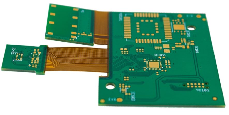
A flexible rigid PCB, also known as a rigid-flex PCB, is a hybrid circuit board that combines elements of both rigid and flexible substrates into a single unit. This design allows the board to bend and fold while maintaining structural stability in specific areas. The evolution of flexible rigid PCB technology stems from the need for compact, lightweight, and high-reliability electronic solutions in increasingly complex devices. Over the years, this PCB type has gained widespread adoption across various industries, including aerospace, medical devices, automotive systems, and consumer electronics. Unlike traditional rigid PCBs, which are entirely stiff, or flexible PCBs, which lack structural support, a flexible rigid PCB provides the best of both worlds—mechanical durability where needed and flexibility for space-saving and dynamic applications. This combination not only enhances design freedom but also reduces interconnection issues, making it a go-to choice for cutting-edge electronics.
Structure and Types of Flexible Rigid PCB
A flexible rigid pcb integrates rigid FR-4 sections with flexible polyimide areas, bonded together with specialized adhesives and copper foils. The rigid regions provide mechanical support for component placement and high-density routing, while the flexible zones allow bending and folding without compromising electrical integrity. Layers are laminated in a controlled, temperature-and-pressure process: copper foil is first laminated to each substrate, coverlay is applied over flex regions, then alternating rigid and flex cores are stacked and pressed to form a unified board.
Common Types of Flexible Rigid PCB Structures and Designs
-
Single-Sided Rigid-Flex
-
One rigid layer bonded to one flexible layer
-
Ideal for simple bend-around designs
-
-
Double-Sided Rigid-Flex
-
Rigid core with flex on both sides
-
Supports moderate complexity and bi-directional flex
-
-
Multilayer Rigid-Flex
-
Multiple rigid and flex layers stacked alternately
-
Enables high-density interconnects and complex routing
-
Example Structure
A typical multilayer design might include:
-
Rigid Layer (Signal)
-
Adhesive and Flex Core (Coverlay on both sides)
-
Inner Rigid Core (Ground Plane)
-
Adhesive and Flex Core
-
Outer Rigid Layer (Power Plane)
In practice, designers often refer to a stackup diagram (e.g., Figure 1) showing each layer’s thickness and material, clearly marking rigid and flex regions and indicating bend radii in the flex zones.
Materials Used in Flexible Rigid PCB
In a flexible rigid pcb, material selection is critical to achieving both bendability and structural integrity. The board is composed of distinct flexible and rigid substrates, each chosen for their unique properties.
Flexible Layers
-
Polyimide (PI): Renowned for its exceptional thermal stability (up to 400 °C) and chemical resistance, PI is the most common flex substrate.
-
Polyester (PET): A lower-cost alternative to PI, PET offers good dimensional stability and moderate thermal performance (up to 150 °C), suitable for less demanding applications.
Rigid Layers
-
FR-4: The industry-standard rigid laminate made from woven fiberglass and epoxy resin. FR-4 delivers excellent mechanical strength, dielectric properties, and affordability.
-
Rogers Materials: High-frequency laminates (e.g., Rogers 4350B) provide superior dielectric constant control and low loss, ideal for RF/microwave sections in a rigid-flex design.
Key Materials
-
Copper Foil: Typically 1 oz (35 µm) to 2 oz (70 µm) thickness; rolled annealed (RA) foil is preferred in flex zones for its ductility.
-
Adhesives: Thermosetting acrylic or epoxy adhesives bond rigid and flex layers, ensuring peel strength and reliability under thermal cycling.
-
Coverlay: A PI-based cover film laminated over flex areas to protect traces from moisture, abrasion, and stress.
Impact on Performance
Choosing the right combination of PI or PET flex cores, FR-4 or Rogers rigid cores, and compatible adhesives/coverlays directly affects:
-
Flexibility: PI with RA copper allows tight bend radii without trace fatigue.
-
Durability: High-quality adhesives maintain adhesion through repeated flex cycles.
-
Thermal Resistance: Rogers materials and PI substrates withstand higher operating temperatures, enabling robust performance in harsh environments.
Rigid-Flex PCB Design Guidelines for Flexible Rigid PCB
When designing a flexible rigid pcb, engineers must balance circuit integrity with mechanical flexibility. Follow these guidelines to optimize performance and reliability:
Routing Best Practices
-
Avoid 90° bends: Use 45° or curved traces to minimize impedance discontinuities and prevent stress concentrations at corners.
-
Maintain consistent spacing: Keep trace-to-trace and trace-to-edge clearances uniform, especially through bend zones, to avoid delamination and electrical shorts.
-
Use teardrops: Add teardrop fillets at pad-to-trace junctions to reinforce high-stress areas.
Trace Design in Bend Zones
-
Center traces: Route all copper at the neutral axis (center) of the flex layer to reduce tensile strain during bending.
-
Limit copper coverage: Keep bend areas as thin as possible, with narrow traces and minimal copper pour to allow smooth flexing.
Static vs. Dynamic Flexing
-
Static flex: For one-time or occasional bends, use standard PI flex cores with conservative bend radii (≥10× flex thickness).
-
Dynamic flex: For repeated motion, choose RA (rolled annealed) copper and increase bend radii (≥20× flex thickness) to withstand millions of cycles.
Avoiding Stress Concentration
-
Smooth transitions: Gradually taper rigid-to-flex interfaces and use chamfered stiffener edges.
-
Reinforce high-stress points: Add coverlay reinforcements or strain reliefs at connector terminations.
DFM (Design for Manufacturability) Tips
-
Standardize layer stackups: Use common flex and rigid core thicknesses to streamline lamination.
-
Specify tooling tolerances: Clearly call out drill-to-copper clearances and minimum annular ring sizes.
-
Collaborate early with the fabricator: Validate bend radii, material choices, and stackup to ensure manufacturability and yield.
Typical Flexible Rigid PCB Stackups
A well-defined flexible rigid pcb stackup ensures signal integrity, mechanical stability, and ease of manufacturing. Below are common approaches:
Single-Layer Stackup
-
Structure: One rigid FR-4 core bonded to a single polyimide flex layer with coverlay.
-
Use Case: Simple bend applications where only one side requires routing flexibility.
-
Example:
-
Rigid FR-4 (1.6 mm)
-
Adhesive layer
-
Flex PI core (0.1 mm) with coverlay
-
Copper foil (35 µm)
-
Multilayer and Alternating Stack Structures
-
Multilayer Rigid-Flex: Alternating rigid and flex cores to support complex routing and multiple power/ground planes.
-
Typical Build:
-
Outer rigid signal layers (2 × 1 oz Cu)
-
Adhesive + Flex PI + coverlay
-
Inner rigid ground/power plane
-
Adhesive + Flex PI + coverlay
-
Outer rigid signal layer
-
-
Benefit: High-density interconnects and controlled impedance across both rigid and flex sections.
Managing Rigid-to-Flex Transition Zones
-
Gradual Layer Count Changes: Step down copper and dielectric thickness in stages to minimize stress.
-
Tapered Adhesive Areas: Reduce adhesive overlap to prevent delamination.
-
Stiffener Integration: Add localized stiffeners (e.g., FR-4 or stainless steel) to support connectors without compromising bend areas.
EMI/EMC Shielding Layer Placement
-
Ground Planes in Flex: Include an inner flex plane dedicated to ground to form a continuous shield.
-
Shield Coverlay: Apply a conductive polymer coverlay over flex regions for additional EMI protection.
-
Via Stitching: Stitch vias between ground planes in rigid and flex areas to maintain a low-inductance return path and minimize emissions.
Manufacturing Overview of Flexible Rigid PCB
Manufacturing a flexible rigid pcb involves precise coordination of rigid and flex processes to achieve a unified, high-performance board.
Key Process Steps
-
Drilling: Use mechanical drilling for rigid sections and laser drilling for flex cores to prevent delamination and burring.
-
Lamination: Stack rigid FR-4 and polyimide flex cores with adhesive films under controlled temperature and pressure to form a single laminate.
-
Imaging: Employ sequential photolithography for each copper layer, ensuring accurate pattern transfer on both rigid and flex substrates.
-
Surface Finish: Apply finishes such as ENIG (Electroless Nickel Immersion Gold) or OSP (Organic Solderability Preservative), selecting chemistries compatible with flex areas to avoid cracking.
Special Considerations for Flex-Rigid Integration
-
Coverlay Alignment: Precisely register coverlay over flex zones to protect traces and maintain bend reliability.
-
Racking and Support: Use custom fixtures during lamination and plating to support flex areas and maintain uniform pressure.
Quality Control
-
AOI (Automated Optical Inspection): Detect surface defects, misregistration, and soldermask issues.
-
X-Ray Inspection: Verify internal layer alignment and detect voids in flex-rigid transitions.
-
Electrical Testing: Perform flying probe or ICT (In-Circuit Testing) to ensure continuity, isolation, and impedance compliance.
Advantages and Challenges of Flexible Rigid PCB
A flexible rigid pcb combines the strengths of both rigid and flexible circuit technologies, making it an ideal solution for compact, high-performance electronic systems. However, it also introduces specific design and production challenges that must be carefully managed.
Advantages
- Space-Saving, Lightweight Design
A flexible rigid pcb enables engineers to eliminate bulky connectors and cables between rigid boards by integrating all circuits into a single, foldable structure. This reduces the overall weight and footprint—critical for portable, wearable, and aerospace applications. - Enhanced Reliability and Signal Integrity
By minimizing solder joints and interconnects, a flexible rigid pcb reduces potential failure points. The unified structure improves signal paths, supports controlled impedance, and enhances overall electrical performance, especially in high-speed and RF circuits. - Resistance to Vibration and Movement
The flexible layers in a flexible rigid pcb absorb mechanical stress, making the board more resistant to vibration, shock, and thermal cycling. This is essential for automotive, defense, and industrial applications that demand long-term durability.
Challenges
- Higher Cost
Manufacturing a flexible rigid pcb involves more expensive materials (e.g., polyimide, RA copper) and advanced processes like multi-stage lamination and laser drilling. This leads to a higher unit cost compared to traditional PCBs. - More Complex Design and Fabrication
Designing a flexible rigid pcb requires careful consideration of bend radii, stackup transitions, and mechanical strain. It also involves coordination between electrical and mechanical engineers, increasing design time and complexity. - Requires Advanced Manufacturing Capabilities
Not all PCB manufacturers can handle flexible rigid pcb production. Specialized equipment, cleanroom environments, and experience in handling delicate flex layers are essential to ensure consistent quality and yield.
Leading Flexible Rigid PCB Manufacturers
In the competitive market for flexible rigid pcb solutions, several manufacturers distinguish themselves through advanced capabilities, quick turnarounds, and extensive design support:
-
PCBWay – PCBWay offers a comprehensive Rigid-Flex overview, including turnkey prototyping and small-batch production. Their platform supports custom stackups, fast quoting, and detailed DFM feedback to streamline flexible rigid pcb projects.
-
Sierra Circuits / ProtoExpress – Known for their Flex and Rigid-Flex PCB services, ProtoExpress provides rapid prototypes with laser-drilled vias, class-leading tolerances, and coverlay options. Their expertise ensures reliable performance in both static and dynamic flex applications.
-
MCL – On the MCL blog “Rigid vs Flexible,” you’ll find in-depth comparisons of material choices and design strategies. MCL’s manufacturing capabilities encompass up to 16-layer rigid-flex constructions, with controlled impedance and advanced surface finishes.
-
Hemeixin – Specializing in Long Flex & Rigid-Flex PCBs, Hemeixin offers custom polyimide laminates and RA copper foils. Their production lines accommodate tight bend radii and high-cycle flex requirements essential for wearable and medical devices.
-
Excello Circuits – Excello provides rigid-flex solutions with up to 10 layers, automated optical inspection, and quick-turn delivery. Their process control ensures consistent quality across both rigid and flex zones.
-
PCBCart – PCBCart’s Flex-Rigid Services include multilayer stackup design, impedance control, and surface finishes like ENIG. Their online quoting tool and engineering support simplify complex flexible rigid pcb designs.
Conclusion & Future Trends of Flexible Rigid PCB
The flexible rigid pcb has evolved from a niche technology into an essential component for high-density, high-reliability electronic applications. Its unique combination of flexibility and mechanical strength addresses the complex challenges faced in modern device design, enabling compact, lightweight, and robust solutions. As industries push toward miniaturization and enhanced performance, the demand for flexible rigid pcb solutions continues to grow rapidly.
Looking ahead, sectors such as 5G telecommunications, wearable technology, aerospace, medical devices, and automotive electronics are expected to drive significant growth in flexible rigid pcb adoption. These applications require not only space-saving form factors but also reliable signal integrity and durability under mechanical stress.
Future advancements will increasingly integrate flexible rigid pcb designs with HDI (High-Density Interconnect) techniques and high-speed signal routing, leveraging advanced materials like improved polyimides and low-loss laminates. This integration will further enhance performance and expand the possibilities for next-generation electronics across diverse industries.

