
The Role of DNP Lead Frame for Miniaturized in Packaging
Semiconductor packaging plays a crucial role in the electronics industry, as it protects the delicate microchips while ensuring reliable electrical connections between the chip and external components. As the demand for smaller, more efficient electronic devices continues to grow, the importance of miniaturized semiconductor packaging has become more evident. In this rapidly evolving field, DNP (Dai Nippon Printing Co., Ltd.) stands out for its innovation and leadership. DNP has developed cutting-edge solutions that address the challenges of miniaturization, particularly with its “DNP Lead Frame for Miniaturized” technology. This advanced lead frame technology enables the production of compact, high-performance semiconductor packages that meet the strict requirements of modern electronic applications. The purpose of this article is to delve into DNP’s “Lead Frame for Miniaturized” technology, exploring its key features, applications, and the critical role it plays in the semiconductor industry’s ongoing drive toward miniaturization and enhanced device performance.
What is a Lead Frame? Understanding the Role of DNP Lead Frame for Miniaturized Applications
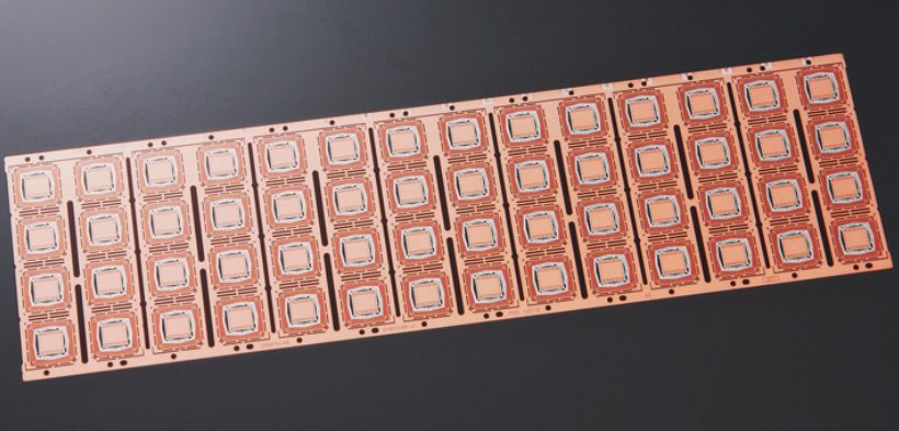
A Lead Frame is a vital component in semiconductor packaging, acting as the physical structure that supports the semiconductor chip and provides the necessary electrical connections between the chip and external circuits. Typically made from metal, the Lead Frame is used to connect the microchip’s bonding pads to the package’s external leads, ensuring proper signal and power transmission. This connection is critical for the chip to function properly within an electronic device.
Lead Frames work by holding the chip in place and providing pathways for the electrical signals to flow from the chip to the outside world. In traditional packaging, Lead Frames are larger and allow for more space to route these connections. However, as the demand for smaller, more efficient devices increases, miniaturized semiconductor packaging has become essential. In this context, DNP Lead Frame for Miniaturized applications plays a significant role by enabling the reduction in package size while maintaining high reliability and performance.
The growing demand for miniaturized packages is driven by the need for compact electronic devices such as smartphones, wearables, and automotive electronics. DNP Lead Frame for Miniaturized solutions are engineered to meet these demands, providing high-density, reliable connections in smaller form factors. This miniaturization allows for enhanced device performance while minimizing space, making it a crucial technology for the future of electronics.
DNP’s Innovations in Miniaturized Lead Frame Technology: The Power of DNP Lead Frame for Miniaturized Applications
DNP (Dai Nippon Printing Co., Ltd.) is a recognized leader in the field of semiconductor packaging, with extensive expertise in the design and manufacturing of Lead Frames. Leveraging decades of experience, DNP has honed its ability to create advanced solutions for both traditional and miniaturized packaging needs. Their DNP Lead Frame for Miniaturized applications showcases cutting-edge technology designed to meet the increasingly stringent demands of modern semiconductor products.
DNP’s miniaturized Lead Frame technology plays a crucial role in pushing the boundaries of smaller, more efficient electronic devices. With the ever-growing trend of miniaturization in the semiconductor industry, DNP Lead Frame for Miniaturized solutions ensure that packages can be both compact and highly reliable. By focusing on key attributes such as size reduction, enhanced thermal performance, and electrical efficiency, DNP is able to offer solutions that are perfectly suited for modern electronic applications like smartphones, wearable devices, and automotive electronics.
Some of the key benefits of DNP Lead Frame for Miniaturized technology include:
- Enhanced Reliability: DNP’s miniaturized Lead Frames are designed to withstand extreme environmental conditions, offering long-lasting performance and reducing the risk of failures due to thermal cycling or mechanical stress.
- Reduced Package Size: DNP’s design optimizations allow for even smaller semiconductor packages without compromising on performance, which is essential for today’s compact devices.
- Improved Thermal Management: Thermal management is crucial in smaller devices where space is limited. DNP’s advanced Lead Frames incorporate superior heat dissipation features to ensure chips remain cool even in high-performance applications.
One of DNP’s standout features is its unique manufacturing process and material selection. By using high-quality materials that offer better electrical conductivity, mechanical strength, and thermal resistance, DNP Lead Frame for Miniaturized products outperform many competitors in the market. Furthermore, DNP’s precision manufacturing ensures that each Lead Frame is optimized for performance, providing consistent quality and reliability across high-volume production runs.
Compared to other players in the semiconductor packaging industry, DNP stands out with its deep expertise in material science, advanced manufacturing technologies, and custom-tailored solutions. The combination of these factors allows DNP Lead Frame for Miniaturized to address the most demanding needs of modern electronics, offering a competitive edge in both innovation and reliability.
Applications of DNP’s Miniaturized Lead Frames: Powering Key Industries with DNP Lead Frame for Miniaturized Solutions
DNP Lead Frame for Miniaturized technology is revolutionizing the semiconductor packaging industry, providing key industries with the essential components needed to meet the demands of today’s compact, high-performance devices. Several industries benefit significantly from DNP’s innovative solutions, including automotive electronics, consumer electronics, telecommunications, and more.
Automotive Electronics
The automotive industry is increasingly relying on smaller, more reliable semiconductor components to power advanced technologies such as autonomous driving, electric vehicles (EVs), and in-vehicle infotainment systems. DNP Lead Frame for Miniaturized offers automotive manufacturers a compact yet highly reliable packaging solution for critical electronic components, such as sensors, control units, and communication modules. These components must operate flawlessly under harsh conditions, including temperature fluctuations, vibrations, and humidity. DNP’s miniaturized Lead Frames excel in these environments, providing long-term performance and ensuring that electronic systems function safely and efficiently.
Consumer Electronics
Consumer electronics, such as smartphones, wearables, and smart home devices, demand cutting-edge technology that can fit into increasingly smaller and thinner designs without compromising on performance. DNP Lead Frame for Miniaturized plays a crucial role in this sector by enabling high-density, small-form-factor packages that provide optimal functionality without increasing device size. The miniaturized nature of these Lead Frames allows manufacturers to pack more features, such as powerful processors and multi-functional sensors, into compact devices like smartphones and smartwatches. The reliability and efficiency of DNP’s technology ensure that these devices perform seamlessly over their lifespan.
Telecommunications
The telecommunications industry, especially with the roll-out of 5G networks, requires high-performance, compact, and efficient semiconductor devices to meet the demands of faster speeds and lower latency. DNP Lead Frame for Miniaturized supports the creation of smaller and more efficient communication modules, such as base station components, routers, and RF (radio frequency) modules. The miniaturized Lead Frames help reduce the overall size of these components while enhancing their electrical performance and thermal management capabilities. DNP’s solutions contribute to the development of next-generation telecommunications equipment that is both reliable and space-efficient.
Specific Use Cases and Product Examples
- Smartphone Chips: DNP’s Lead Frame for Miniaturized technology is used in the packaging of critical smartphone components, such as power management ICs (integrated circuits) and processors. These components need to be both small and reliable, offering superior heat dissipation and electrical connectivity in a space-constrained environment. DNP’s packaging solutions help manufacturers create smartphones that are thinner, faster, and more powerful.
- Wearable Devices: Smartwatches and fitness trackers are other products that benefit from DNP’s miniaturized Lead Frames. These devices require semiconductor packages that can withstand continuous movement and environmental stress while maintaining compactness. DNP Lead Frame for Miniaturized solutions provide the necessary structural integrity and electrical performance, ensuring that these wearables remain functional and reliable over time.
- Electric Vehicle (EV) Sensors: In electric vehicles, DNP’s technology is utilized to package sensors that monitor battery health, temperature, and other critical parameters. These sensors must be small, robust, and capable of operating in high-temperature environments, making DNP Lead Frame for Miniaturized technology an ideal solution. By enabling the creation of more compact, efficient, and reliable sensor packages, DNP contributes to the performance and safety of EVs.
Through these specific applications, DNP demonstrates how its Lead Frame for Miniaturized technology supports key industries in achieving the balance between miniaturization, performance, and reliability. As demand for smaller, more efficient devices continues to rise, DNP’s solutions will remain at the forefront of driving innovation in semiconductor packaging across various sectors.
Advantages of DNP Lead Frames: Key Benefits of DNP Lead Frame for Miniaturized Applications
DNP Lead Frame for Miniaturized technology offers several distinct advantages that set it apart in the semiconductor packaging industry. These benefits make DNP’s solutions ideal for a wide range of applications, from consumer electronics to automotive systems. Let’s explore the key advantages that DNP Lead Frame for Miniaturized technology brings to the table:
High Reliability: Performance in Extreme Environments
One of the most critical factors in semiconductor packaging is reliability, especially in demanding environments. DNP Lead Frame for Miniaturized excels in this area by offering exceptional durability under extreme conditions. Whether it’s high temperatures, humidity, mechanical stress, or thermal cycling, DNP’s miniaturized Lead Frames are designed to withstand the rigors of harsh operating environments. This makes them particularly well-suited for applications in automotive electronics, industrial devices, and aerospace systems, where failure is not an option. The robustness of DNP’s technology ensures that packaged components maintain long-term reliability, reducing the likelihood of failure and ensuring that devices function smoothly over their lifespan.
Miniaturization and Efficiency: Achieving Smaller Sizes Without Sacrificing Performance
As demand for smaller, more powerful electronic devices grows, DNP Lead Frame for Miniaturized provides a solution that enables the creation of compact packages without compromising on performance. The technology allows semiconductor manufacturers to create smaller and more efficient packages that maximize space while maintaining high electrical performance. This is especially crucial in the consumer electronics market, where devices like smartphones and wearables are becoming increasingly thinner and more feature-packed. DNP Lead Frame for Miniaturized ensures that these devices continue to deliver superior performance, including faster processing speeds, enhanced signal reliability, and better heat management, despite their reduced size.
Cost-Effectiveness: Striking the Right Balance Between Cost and Performance
Cost is a significant consideration in any manufacturing process, especially when working with high-volume production runs. DNP Lead Frame for Miniaturized technology offers a cost-effective solution by striking a balance between affordability and performance. DNP’s advanced manufacturing processes and material choices allow for the production of high-quality Lead Frames at competitive prices, ensuring that manufacturers can meet market demands without exceeding their budget. Compared to traditional methods, DNP’s miniaturized Lead Frames provide substantial cost savings in both production and assembly, allowing companies to maintain profitability while still delivering cutting-edge technology to consumers.
Customizability: Tailored Solutions to Meet Specific Needs
Every customer has unique requirements when it comes to semiconductor packaging. DNP’s ability to provide tailored solutions is another key advantage of its miniaturized technology. Whether a client needs a specific package size, material type, or additional features such as enhanced thermal dissipation or electrical performance, DNP can customize its Lead Frames to meet these needs. This level of flexibility is essential for industries like automotive, telecommunications, and consumer electronics, where different applications require specific packaging solutions. By working closely with clients to understand their unique challenges, DNP ensures that each Lead Frame for Miniaturized is optimized for its intended use, providing the best possible performance and value.
DNP Lead Frame for Miniaturized technology offers a combination of high reliability, miniaturization, cost-effectiveness, and customizability, making it an ideal solution for modern semiconductor packaging needs. These advantages make DNP’s Lead Frames a go-to choice for industries that require small, efficient, and reliable packaging for their electronic components.
Industry Trends and Future Outlook: The Path Forward with DNP Lead Frame for Miniaturized Solutions
The semiconductor packaging market is undergoing significant transformation, driven by a relentless demand for smaller, more efficient, and highly reliable electronic devices. As technology evolves, there is a clear movement toward miniaturization—smaller, lighter components that offer higher performance and lower power consumption. This trend is particularly prominent in industries like consumer electronics, automotive, telecommunications, and IoT (Internet of Things), where space constraints are critical, and the need for advanced capabilities in compact devices is ever-growing. DNP Lead Frame for Miniaturized technology is positioned at the forefront of these developments, enabling companies to meet these new challenges with advanced, high-performance packaging solutions.
Current Trends in the Semiconductor Packaging Market
The current landscape of the semiconductor packaging market is focused on achieving high-performance packaging in increasingly smaller form factors. Some of the major trends include:
- Miniaturization: With the rapid evolution of smartphones, wearables, and other compact devices, there is a strong push for smaller and thinner packaging solutions. DNP Lead Frame for Miniaturized addresses this by offering packages that reduce space without compromising on functionality or performance.
- Increased Demand for Reliability: As devices become smaller and more complex, the need for reliable, durable components becomes more critical. In automotive electronics, for example, components need to perform flawlessly in harsh conditions, from high heat to mechanical stress. DNP’s technology supports these reliability requirements with robust designs that can withstand extreme environments.
- Thermal Management: As devices become smaller, managing heat dissipation has become increasingly important. The demand for more efficient thermal management solutions is growing, and DNP Lead Frame for Miniaturized helps solve this challenge by enabling better heat conduction through advanced materials and designs.
These trends show a clear direction for the future of semiconductor packaging: smaller, faster, and more reliable solutions are required across nearly every industry. DNP’s Lead Frame for Miniaturized technology is perfectly aligned with these industry needs, ensuring that they remain a competitive leader in the market.
DNP’s Alignment with Trends and Competitive Edge
DNP has successfully aligned itself with the ongoing trends in the semiconductor packaging market by continuously innovating and improving its solutions. Through its deep expertise in materials science, advanced manufacturing processes, and custom design capabilities, the company is able to stay ahead of the competition.
One key way DNP maintains its competitive edge is through ongoing research and development (R&D) investments, which allow the company to stay at the forefront of emerging packaging technologies. By constantly refining their manufacturing techniques and exploring new materials, DNP ensures that their miniaturized Lead Frames not only meet current market demands but also anticipate future needs. The company’s focus on improving thermal management, electrical efficiency, and mechanical reliability helps ensure that DNP Lead Frame for Miniaturized products continue to offer value in increasingly complex and demanding applications.
DNP has built strong relationships with clients across multiple industries, offering customized solutions that cater to specific performance requirements. This customer-centric approach allows DNP to deliver highly optimized packages that meet the exact needs of their clients, further solidifying their leadership in the semiconductor packaging sector.
Future Directions: Potential Breakthroughs in Packaging Technologies
Looking to the future, DNP Lead Frame for Miniaturized technology is poised to evolve even further with potential breakthroughs in several areas:
- Advanced Materials: DNP is likely to continue exploring new materials that enhance the electrical and thermal properties of Lead Frames. This could include the use of advanced alloys or composite materials that allow for even smaller, more efficient packages with enhanced performance characteristics.
- 3D Packaging: One of the most exciting developments in semiconductor packaging is the advent of 3D packaging, which allows multiple layers of semiconductor components to be stacked vertically. DNP Lead Frame for Miniaturized could evolve to support 3D packages, enabling even greater miniaturization and higher performance in applications like high-performance computing and AI processors.
- Integration of New Technologies: With the rise of technologies like 5G, autonomous driving, and edge computing, the need for high-speed, high-reliability semiconductor components will only increase. DNP is well-positioned to leverage these trends, developing new packaging solutions that incorporate RF (radio frequency) components, sensors, and other cutting-edge technologies into miniaturized packages.
- Sustainability: As sustainability becomes an increasing concern across all industries, DNP may look to develop eco-friendly packaging solutions. This could involve the use of recyclable materials, energy-efficient manufacturing processes, or reducing the carbon footprint of semiconductor packaging.
DNP’s technology is not just aligned with current trends but is also positioned for the future, ready to meet the next generation of challenges in the semiconductor packaging market. Through continuous innovation, a deep understanding of customer needs, and a commitment to advancing packaging technologies, the company is set to remain a key player in the semiconductor industry as it evolves toward even smaller, faster, and more efficient devices.

