
The Role of Copper Leadframe Substrate in Packaging
A Leadframe is a crucial element in semiconductor packaging, providing the physical structure that holds and connects the semiconductor chip to external electrical contacts, while also enabling the transfer of signals and power. Over time, leadframes have evolved from basic designs to more complex forms, supporting the growing demands of miniaturized and high-performance electronic devices. A Substrate, on the other hand, serves as the supporting base for the chip, offering mechanical stability and facilitating electrical connections to the leadframe. While the leadframe focuses on structural integrity and electrical paths, the substrate also aids in heat dissipation. Copper, chosen for its superior thermal conductivity and electrical conductivity, plays a key role in leadframe technology. The Copper Leadframe Substrate combines these unique properties, ensuring efficient performance and enhanced reliability in semiconductor packaging.
Materials Used in Copper Leadframe Substrate
When it comes to Copper Leadframe Substrate, the materials used in leadframe construction play a crucial role in ensuring the performance and reliability of semiconductor devices. Among these materials, copper stands out as the primary choice due to its superior properties.
Copper as the Primary Material
Copper is highly preferred in leadframe construction because of its exceptional ductility, low electrical resistance, and high thermal conductivity. These properties make it ideal for ensuring efficient electrical connections and effective heat dissipation. Ductility allows copper to be easily molded into complex shapes, making it suitable for the precise demands of modern semiconductor packaging. Its low resistance ensures minimal power loss, while its heat dissipation capabilities help in managing the heat generated by the semiconductor during operation, preventing overheating and damage to sensitive components. For these reasons, copper has become the material of choice for Copper Leadframe Substrate in a wide range of electronic applications.
Other Materials
While copper remains the most commonly used material, other materials and alloys are also utilized in leadframe construction, especially when specific performance characteristics are needed.
-
Copper-Tungsten Alloy: This alloy combines the high thermal conductivity of copper with the strength and durability of tungsten. It is particularly useful in high-power applications where thermal management is critical. Copper-tungsten leadframes are often used in power electronics, such as in automotive and industrial systems, where heat generation is significant.
-
Copper-Nickel Alloy: Copper-nickel leadframes offer enhanced corrosion resistance and better mechanical properties, making them suitable for applications in harsh environments, such as outdoor or high-humidity settings. These leadframes are commonly used in electronics exposed to challenging conditions, including some military and aerospace applications.
-
Other Composites and Alloys: Materials like Copper-Beryllium and Copper-Molybdenum alloys are also used in specialized leadframes, especially where enhanced strength or specific thermal properties are required for high-performance semiconductors.
Each of these materials is chosen based on the specific requirements of the Copper Leadframe Substrate, ensuring that the final package meets the performance, durability, and thermal needs of the semiconductor device.
Leadframe vs. Substrate in Copper Leadframe Substrate
In semiconductor packaging, both the Copper Leadframe Substrate and the substrate serve critical roles, but they function in distinct ways, each supporting the chip in different capacities. Understanding the functional differences, design considerations, and manufacturing complexities of these components is essential to grasp how they work together to enhance the performance of semiconductor devices.
Functional Differences of Copper Leadframe Substrate
The leadframe primarily serves as a conductive path and physical frame. It provides the electrical connections between the semiconductor chip and the external circuitry by linking the internal contacts of the chip to the external pins or pads. The leadframe also provides structural support, holding the chip in place and ensuring that it stays securely connected during operation. In Copper Leadframe Substrate, copper’s excellent thermal and electrical properties ensure efficient heat management and reliable conductivity.
The substrate functions as the base layer that supports the semiconductor chip. It provides a stable foundation for mounting the chip and facilitates the necessary interconnections between the chip and the leadframe. The substrate is essential in connecting the chip’s internal pads to the leadframe’s external leads through wire bonds or other bonding techniques. Additionally, the substrate plays a significant role in heat dissipation, often incorporating materials or features designed to prevent the chip from overheating.
Design Considerations for Copper Leadframe Substrate
When considering Copper Leadframe Substrate designs, the roles of the leadframe and substrate are carefully balanced. The leadframe is more focused on structural integrity and electrical connection. It must be designed to withstand the mechanical stress of packaging processes and electrical stresses during the operation of the semiconductor. Its function is largely to ensure that the chip is connected reliably to the outside world without causing overheating or performance issues.
The substrate has a more complex role. It must provide both electrical connections and heat dissipation. Besides being a physical base for the chip, the substrate also acts as a medium for conducting heat away from the chip, ensuring that the semiconductor operates within safe thermal limits. This is particularly important in high-performance or high-power applications where heat management is critical. Materials with high thermal conductivity, such as Copper Leadframe Substrate, are often incorporated into the substrate for effective thermal management.
Cost & Manufacturing of Copper Leadframe Substrate
In terms of cost and manufacturing, the Copper Leadframe Substrate is generally more complex to produce than the substrate. Leadframe manufacturing involves intricate processes such as stamping, molding, and etching, often requiring high precision to ensure reliable electrical and mechanical properties. The use of copper, which is both ductile and thermally conductive, adds additional costs but improves the overall reliability and performance of the semiconductor device.
Substrate manufacturing, while also complex, involves a different set of challenges, including the selection of materials with high thermal and electrical conductivity, as well as the integration of advanced features like heat sinks or via holes for electrical interconnections. Substrates may be more cost-effective than leadframes in some cases, depending on the material and process chosen, but for Copper Leadframe Substrate designs, the combination of materials and techniques used must align with the desired performance outcomes, especially for high-performance devices.
While both the leadframe and substrate are indispensable in semiconductor packaging, their roles, design considerations, and manufacturing processes differ. The Copper Leadframe Substrate combines the best of both, leveraging copper’s exceptional properties for both electrical connections and heat dissipation.
Types of Leadframe Designs in Copper Leadframe Substrate
The design of leadframes has evolved significantly to meet the increasing demands of modern semiconductor packaging. In the context of Copper Leadframe Substrate, several types of leadframe designs are used, each tailored to different applications and performance requirements. These designs range from traditional configurations to more compact and specialized variants, reflecting the drive for miniaturization and improved efficiency in electronic devices.
Traditional Leadframe
The traditional leadframe is the foundational design used in semiconductor packaging. It is typically made of copper or copper alloys and provides both mechanical support and electrical connections for the semiconductor chip. There are two main types of traditional leadframes:
-
Flat Leadframe: This is the simplest design, where the leads (electrical connectors) are arranged in a flat, parallel configuration around the perimeter of the chip. The flat leadframe is easy to manufacture and cost-effective, making it suitable for a wide range of applications.
-
Stamped and Etched Leadframe: This type of leadframe is produced through stamping and etching processes, where copper is cut into precise shapes using molds or lasers. The Copper Leadframe Substrate used in this design offers excellent conductivity and thermal properties, and the process allows for more intricate designs than the flat leadframe, accommodating more complex semiconductor devices.
Traditional leadframes are typically used for larger, less miniaturized components where the demands for heat dissipation and electrical connections are less stringent than in smaller, high-performance electronics.
Micro Leadframe
With the rise of miniaturized electronics, the demand for more compact leadframe designs has led to the development of the micro leadframe. These leadframes are significantly smaller in size compared to traditional designs, which is crucial for devices with high-density components, such as mobile phones, wearables, and other portable electronics.
A micro leadframe features fine-pitch leads, allowing for closer spacing between the chip and the external electrical connections. This design enables manufacturers to produce smaller, lighter, and more efficient semiconductor packages, which are critical for meeting the size constraints of modern consumer electronics. The Copper Leadframe Substrate used in micro leadframes ensures that the miniaturized designs maintain high electrical and thermal performance, which is essential for devices that require both power efficiency and compact form factors.
The advantages of micro leadframes include:
- Smaller package sizes, suitable for portable devices.
- Improved performance in terms of electrical conductivity and heat management.
- Better space utilization, allowing for more compact, feature-rich electronics.
Other Leadframe Variants
Beyond traditional and micro leadframes, several other Copper Leadframe Substrate designs are tailored to specific applications that require unique packaging configurations. Some of these include:
-
Dual-In-Line Package (DIP): The DIP leadframe is one of the most widely used designs in through-hole mounted electronic components. The leads extend from opposite sides of the chip, and the component can be inserted into a corresponding socket or PCB. This design is used in applications where components need to be easily replaceable or reworked, such as in older electronics.
-
Ball Grid Array (BGA): The BGA leadframe design is used in high-performance applications like computers and smartphones, where space and heat dissipation are critical. Instead of traditional leads, the BGA uses an array of solder balls that connect the chip directly to the PCB. This design allows for a much higher pin count and improved heat management, making it ideal for high-speed, high-performance applications.
-
Chip-on-Lead (COL): The COL design is a more advanced approach that allows the chip to be directly attached to the leadframe, rather than using traditional wire bonding. This design reduces the overall size of the package and improves electrical performance by minimizing the distance between the chip and the leadframe. The Copper Leadframe Substrate in this design is particularly advantageous for reducing signal loss and improving overall efficiency.
Each of these leadframe variants is chosen based on specific requirements such as electrical performance, heat dissipation, space constraints, and manufacturability. The versatility of the Copper Leadframe Substrate in different leadframe designs highlights its importance in supporting a wide array of electronic devices, from legacy systems to cutting-edge, miniaturized technologies.
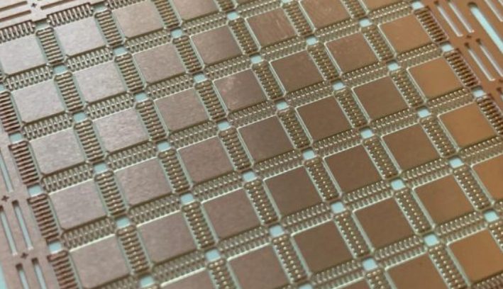
Manufacturing Process of Copper Leadframes in Copper Leadframe Substrate
The manufacturing process of Copper Leadframe Substrate involves several critical steps that ensure high-performance and reliable semiconductor packaging. From selecting the right materials to integrating the leadframe with the semiconductor die, each stage plays a crucial role in the final performance and durability of the semiconductor component. Here, we delve into the key processes that define the creation of a Copper Leadframe Substrate.
Materials Selection and Preparation
The foundation of any Copper Leadframe Substrate lies in the careful selection of materials. Copper is the material of choice due to its superior electrical conductivity and thermal conductivity, which are essential for ensuring efficient power transfer and heat dissipation in semiconductor devices. Copper’s mechanical properties, such as ductility, allow it to be easily shaped and molded into the required configurations during manufacturing, while its low resistance ensures minimal power loss.
To prepare copper for the leadframe process, it is sourced in sheets or coils that are then subjected to various treatments to improve its strength and surface properties. In some cases, copper alloys like copper-nickel or copper-tungsten may be used depending on specific performance requirements such as corrosion resistance or thermal conductivity.
Stamping, Etching, and Molding Processes
The stamping, etching, and molding processes are the key techniques used to form the Copper Leadframe Substrate from raw copper material. These methods allow for the precise shaping of the leadframe and ensure that the final product meets strict industry standards for both electrical and mechanical performance.
-
Stamping: The copper sheet is placed into a die and subjected to high-pressure stamping to create the basic outline of the leadframe. This method enables the mass production of leadframes with consistent shape and size, which is crucial for maintaining quality and uniformity in semiconductor packaging.
-
Etching: After stamping, additional steps like etching may be used to refine the leadframe’s structure. During this process, the copper is subjected to chemical treatments that etch away unwanted portions, leaving behind intricate patterns that correspond to the specific design of the leadframe. This is particularly important for designs that require precise electrical connections and thin, delicate leads.
-
Molding: In some cases, the Copper Leadframe Substrate may undergo a molding process where the leadframe is encased in a mold to form a protective package around the semiconductor die. This process helps to stabilize the leadframe, especially in advanced packaging techniques such as Chip-on-Lead (COL) or Ball Grid Array (BGA).
Plating and Surface Finishing
Once the leadframe is stamped, etched, and molded, it undergoes a series of plating and surface finishing processes to enhance its durability and prevent corrosion. These coatings are essential for protecting the Copper Leadframe Substrate from environmental factors that could lead to degradation, such as moisture or oxidation.
-
Nickel Plating: One of the most common plating techniques is nickel plating, which provides a corrosion-resistant layer that improves the longevity of the leadframe. Nickel plating also enhances the mechanical strength of the leadframe, ensuring that it can withstand the stresses during assembly and operation.
-
Gold Plating: For high-performance applications, gold plating is often applied to the leads of the Copper Leadframe Substrate. Gold is highly resistant to corrosion and provides excellent electrical conductivity, making it ideal for critical connections where low resistance is required. Gold-plated leadframes are commonly used in advanced semiconductor packaging, including micro leadframes and high-speed applications.
-
Other Surface Finishes: Depending on the application, other surface finishes such as silver, tin, or palladium may be used. These finishes are chosen based on their specific electrical, thermal, and corrosion-resistant properties, ensuring that the leadframe performs optimally throughout the lifespan of the device.
Integration with Semiconductors
The final step in the manufacturing process of the Copper Leadframe Substrate is the integration of the leadframe with the semiconductor die. This process involves carefully aligning the leadframe with the semiconductor and establishing the necessary electrical connections.
-
Die Attach: The semiconductor die is attached to the leadframe using a bonding material, typically epoxy or solder. This adhesive secures the die to the leadframe and ensures proper alignment for the next steps.
-
Wire Bonding: After the die is attached, wire bonding is used to connect the chip’s internal pads to the leads of the Copper Leadframe Substrate. Fine gold or aluminum wires are used to create these electrical connections, which are critical for transferring signals and power between the chip and the external world.
-
Encapsulation: Finally, the entire assembly is often encapsulated in a protective resin or plastic material to shield the semiconductor from physical damage, moisture, and other environmental factors. This final package ensures the chip’s reliability and performance throughout its lifecycle.
The manufacturing process of a Copper Leadframe Substrate involves a combination of material selection, advanced shaping techniques, surface finishing, and precise integration with semiconductor dies. These processes work together to produce a leadframe that not only provides reliable electrical connections but also ensures durability, heat dissipation, and performance in various electronic applications.
Advantages of Copper Leadframe Substrate
The Copper Leadframe Substrate offers several distinct advantages that make it the preferred choice for semiconductor packaging. From its electrical performance to its thermal properties and durability, copper ensures that semiconductor devices operate efficiently and reliably. Let’s explore the key advantages in greater detail.
Electrical Performance
One of the most significant advantages of the Copper Leadframe Substrate is its superior electrical conductivity. Copper outperforms many other metals, such as iron or aluminum, commonly used in leadframe construction. Its low resistance allows for efficient transmission of electrical signals, which is crucial in high-performance electronic applications where signal integrity is paramount.
The exceptional conductivity of copper ensures that the electrical paths between the semiconductor die and the external connections are optimized, minimizing energy losses and improving overall efficiency. For advanced semiconductor packaging, such as micro leadframes or high-speed devices, Copper Leadframe Substrate provides the necessary electrical properties to support fast data transmission and power delivery, making it ideal for use in mobile devices, computers, and other high-frequency applications.
Thermal Performance
Another key advantage of the Copper Leadframe Substrate is its enhanced thermal performance. Semiconductor devices generate significant amounts of heat during operation, and the ability to manage this heat is critical to ensuring the chip’s longevity and optimal performance. Copper’s high thermal conductivity allows it to quickly dissipate heat away from the semiconductor die, preventing the chip from overheating and potentially failing.
When used in semiconductor packaging, Copper Leadframe Substrate ensures that the heat generated by the chip is efficiently transferred to the leadframe and then away from the device, maintaining safe operating temperatures. This is especially important for high-power applications such as power amplifiers, automotive electronics, and industrial systems, where excessive heat can lead to performance degradation or even failure of the chip. The superior heat dissipation properties of copper make it the material of choice for these demanding applications, helping to extend the life of the semiconductor and improve overall system reliability.
Durability and Reliability
The durability and reliability of Copper Leadframe Substrate are another set of significant advantages that contribute to its widespread use in semiconductor packaging. Copper is inherently resistant to corrosion and oxidation, two common factors that can degrade the performance of metal leadframes over time. In environments with exposure to moisture, heat, and other corrosive elements, the copper’s resistance to corrosion ensures that the leadframe maintains its mechanical integrity and electrical conductivity.
In addition to its resistance to corrosion, copper is highly durable and can withstand physical stresses during the packaging process, such as molding, wire bonding, and thermal cycling. This robustness is particularly important for Copper Leadframe Substrate used in rugged applications like automotive electronics, aerospace components, and industrial machinery, where the devices are exposed to harsh conditions, including vibrations, temperature fluctuations, and physical impacts.
The long-term reliability of copper-based leadframes contributes to the overall performance of the packaged semiconductor. With copper’s superior mechanical properties, semiconductor devices can operate for extended periods without degradation in electrical or thermal performance, ensuring consistent functionality and minimizing the need for repairs or replacements.
The Copper Leadframe Substrate offers exceptional electrical performance, thermal efficiency, and durability, making it an ideal choice for a wide range of semiconductor applications. Copper’s superior conductivity and heat dissipation properties ensure that the devices function reliably, while its resistance to corrosion and physical damage enhances the long-term durability and operational lifespan of the components. These advantages are crucial for industries demanding high performance, reliability, and efficiency in their electronic systems.
Applications of Copper Leadframe Substrate
The Copper Leadframe Substrate plays a vital role across a variety of industries, offering high-performance capabilities that meet the demands of modern electronic systems. From consumer electronics to automotive and industrial/military applications, copper-based leadframes are essential for ensuring reliability, efficiency, and longevity. Let’s explore the different sectors where Copper Leadframe Substrate is commonly used.
Consumer Electronics
In consumer electronics, the Copper Leadframe Substrate is integral to a wide range of devices such as mobile phones, laptops, tablets, and wearable gadgets. These devices require high-density, compact packaging for their semiconductors, and copper’s superior electrical conductivity and thermal management properties make it ideal for these applications.
For mobile devices, Copper Leadframe Substrate ensures reliable signal transmission, fast processing, and efficient heat dissipation—all essential features for performance-driven gadgets. Smartphones and tablets, which need to balance power efficiency with compact form factors, benefit from the smaller and more intricate designs of micro leadframes, which maximize space without compromising on performance.
Copper’s resistance to corrosion and its durability ensure that semiconductor components in consumer electronics continue to perform effectively over time, even with constant usage and exposure to environmental factors like moisture or dust.
Automotive Electronics
The Copper Leadframe Substrate is becoming increasingly important in automotive electronics, where reliability, high performance, and thermal efficiency are crucial for both safety and functionality. Automotive microchips, sensors, and control units rely on copper-based leadframes to deliver consistent performance in demanding environments, such as under high temperatures, vibrations, and exposure to harsh weather conditions.
In modern vehicles, systems such as engine control units (ECUs), advanced driver-assistance systems (ADAS), and powertrains rely heavily on semiconductor technology. The Copper Leadframe Substrate ensures that the electronic components in these systems operate effectively, especially for power electronics, where efficient heat dissipation is essential. For example, power modules that manage electric vehicle (EV) battery systems require Copper Leadframe Substrate due to copper’s superior thermal conductivity, which helps to keep the system cool and prevent overheating during operation.
The rugged nature of copper also makes it suitable for the automotive industry, where components must withstand harsh environments, such as temperature fluctuations, vibrations, and exposure to chemicals or moisture. This durability, combined with copper’s excellent electrical properties, makes it indispensable for critical automotive applications.
Industrial and Military
In industrial and military applications, where performance is non-negotiable, the Copper Leadframe Substrate excels by providing the necessary reliability and durability to operate in extreme conditions. These industries often require high-performance semiconductors that can withstand rugged environments, such as harsh temperatures, extreme vibrations, and electromagnetic interference.
-
Industrial applications: Systems used in automation, robotics, and factory machinery rely on Copper Leadframe Substrate for their microprocessors, sensors, and controllers. These systems often operate in harsh environments where heat dissipation is crucial. The Copper Leadframe Substrate ensures that the microelectronics perform consistently, even when exposed to high temperatures, humidity, or physical stress.
-
Military applications: In military and aerospace technology, the performance and reliability of semiconductor components are critical, especially in applications such as radar systems, communication equipment, and guidance systems. The Copper Leadframe Substrate provides robust electrical connections and excellent heat management, ensuring that military systems operate efficiently even in extreme conditions. Additionally, the Copper Leadframe Substrate offers resistance to corrosion, which is essential for equipment used in both land-based and space environments, where reliability and longevity are of paramount importance.
The Copper Leadframe Substrate is also widely used in high-frequency applications, including radar and satellite communication, where signal integrity and low-loss performance are essential. Its ability to handle high currents and voltages, combined with its ability to dissipate heat effectively, makes it an excellent choice for mission-critical systems in these sectors.
The Copper Leadframe Substrate finds applications across a wide range of industries, including consumer electronics, automotive electronics, and industrial/military sectors, due to its superior electrical performance, thermal efficiency, and durability. From mobile devices to automotive control systems and military technology, copper-based leadframes ensure that semiconductor components can meet the demanding requirements of these high-performance applications.
Challenges and Innovations in Copper Leadframe Substrate Technology
As semiconductor technology continues to evolve, the Copper Leadframe Substrate faces a range of challenges and opportunities for innovation. The push for miniaturization and the development of new materials aim to improve performance while meeting stricter environmental and sustainability standards. These advancements are critical to overcoming the limitations of traditional leadframe technology, ensuring that copper-based substrates remain at the forefront of modern electronics. Below, we explore the key challenges and innovations shaping the future of Copper Leadframe Substrate technology.
Miniaturization and Precision
One of the most significant challenges for Copper Leadframe Substrate technology is the ongoing trend toward miniaturization of semiconductor packages. As devices become smaller and more compact, the demand for more intricate and precise leadframe designs increases. Miniaturized devices, such as smartphones, wearable gadgets, and high-performance microelectronics, require Copper Leadframe Substrate that can accommodate smaller footprints without sacrificing electrical and thermal performance.
The shift toward smaller and more intricate semiconductor packages demands higher precision in manufacturing processes, particularly in stamping, etching, and wire bonding. Advanced micro leadframes, which are designed to reduce the space taken up by leads while maintaining efficient electrical and thermal pathways, are becoming increasingly popular. These leadframes need to handle ever-increasing numbers of connections and higher currents while still meeting the demanding performance criteria of modern applications.
With smaller devices, achieving precision in the Copper Leadframe Substrate is crucial, as even minor deviations can lead to faulty connections or insufficient heat dissipation. Research into advanced manufacturing techniques, such as laser etching and fine-pitch bonding, is key to maintaining both high performance and miniaturization. However, these advancements also present challenges in maintaining the structural integrity of copper while keeping costs manageable.
New Materials and Hybrid Leadframes
To enhance the performance of the Copper Leadframe Substrate, there is ongoing research into new materials and hybrid leadframes that combine copper with other metals or composites. While copper remains the primary material due to its excellent electrical conductivity and thermal properties, it can sometimes be limited in certain high-demand applications, especially when dealing with extreme conditions.
- Copper-tungsten alloys are one such innovation, offering enhanced thermal conductivity and mechanical strength, making them ideal for power electronics and high-temperature applications.
- Copper-nickel alloys are also gaining traction for their corrosion resistance, which is essential in automotive, industrial, and marine applications where exposure to moisture and chemicals is common.
In some applications, hybrid leadframes are being developed that combine copper with other materials like ceramic or composite plastics to create multi-material leadframes. These hybrid leadframes aim to improve mechanical stability, thermal management, and cost efficiency while allowing for designs that incorporate both the benefits of copper and the advantages of other materials. The Copper Leadframe Substrate is evolving to integrate multiple materials that work synergistically, especially in miniaturized, high-performance devices like 5G components or electric vehicle (EV) power systems.
Sustainability and Environmental Impact
As environmental concerns and regulatory standards increase, the semiconductor industry is making efforts to improve the sustainability of Copper Leadframe Substrate production. The environmental impact of materials used in semiconductor packaging, such as the extraction and processing of metals like copper, has become a growing concern. As a result, companies are exploring ways to make the leadframe production process more eco-friendly and resource-efficient.
One major focus is reducing energy consumption in the manufacturing of leadframes. Traditional processes such as stamping and etching can be energy-intensive, so innovations in cleaner production technologies are being explored. Techniques like laser cutting or electroforming may offer lower energy requirements while still providing the precision necessary for Copper Leadframe Substrate production.
Recycling is a key consideration in improving the sustainability of copper-based leadframes. Recycling copper from used leadframes and other electronic waste (e-waste) not only reduces the environmental impact of mining and refining new copper but also lowers the cost of raw materials. Efforts to reduce waste during manufacturing and increase recycling rates are essential steps toward making the Copper Leadframe Substrate more sustainable.
Another area of research involves developing biodegradable or environmentally friendly materials that could eventually replace copper or minimize its impact during production. While these alternatives are still in the early stages, innovations in this area could significantly reduce the environmental footprint of Copper Leadframe Substrate production in the future.
The Copper Leadframe Substrate continues to be a cornerstone of modern semiconductor packaging, but it faces several challenges as technology evolves. The ongoing miniaturization of devices, combined with the push for higher performance and eco-friendly production, requires continuous innovation. By exploring new materials, hybrid leadframes, and more sustainable manufacturing practices, the Copper Leadframe Substrate will remain a key component in driving the future of electronics, ensuring that they meet the increasing demands of consumers, industries, and the environment.
FQAs Abut Copper Leadframe Substrate
What is the difference between substrate and Leadframe?
-
Function:
- Leadframe: The leadframe serves as a structural support for the semiconductor chip and provides the necessary conductive paths for electrical signals to flow between the chip and the external circuitry.
- Substrate: The substrate is the base layer that supports the chip, connects it to the leadframe, and ensures reliable electrical connections. It also plays a key role in heat dissipation and stabilizing the chip.
-
Role in Packaging:
- Leadframe: Primarily responsible for external connections and mechanical strength, enabling the chip to interact with the external world.
- Substrate: Acts as a bridge between the chip and the leadframe, facilitating both electrical connectivity and thermal management.
-
Materials:
- Leadframe: Typically made from metals such as copper, copper alloys, or sometimes aluminum.
- Substrate: Usually made from materials like epoxy, ceramic, or polyimide, which provide insulation and structural support for the chip.
What materials are used in lead frames?
-
Copper: The most common material used for leadframes due to its excellent electrical conductivity and thermal conductivity, which help in heat dissipation and efficient signal transfer.
-
Copper Alloys: Materials like copper-tungsten or copper-nickel are used for specific applications requiring enhanced strength, thermal performance, or resistance to corrosion.
-
Nickel: Often used as a plating material to protect the leadframe from corrosion and oxidation.
-
Gold: Sometimes used for the outer layer or as part of the plating to improve conductivity and protect the leadframe.
-
Stainless Steel: Used in some cases for leadframes requiring higher mechanical strength and durability.

