
Transparent PCBs: The Future of Electronics
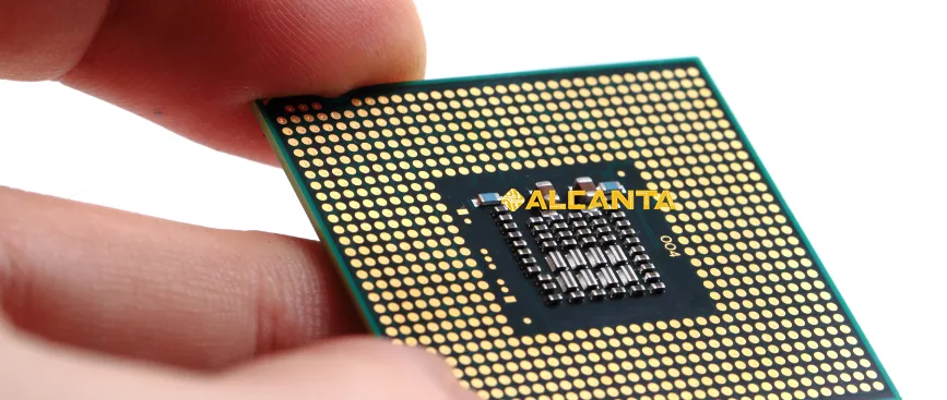
Clear PCB substrate refers to the use of transparent materials as the base for printed circuit boards (PCBs), allowing visibility through the board. The substrate material in PCBs is crucial as it provides mechanical support and electrical insulation. However, with the emergence of transparent substrates, PCBs have entered a new realm of innovation. This blog aims to delve into the significance of substrate materials in PCBs, particularly focusing on transparent options. By exploring the advantages, applications, and manufacturing processes of clear PCBs, readers will gain insights into the future of PCB technology and its potential impact across various industries.
What is Clear PCB Substrate?
Clear PCB substrate refers to the use of transparent materials such as glass or transparent polymers as the base material for printed circuit boards (PCBs). Unlike traditional opaque substrates, clear PCB substrates allow for visibility through the board, offering unique advantages in various applications.
Explanation of Clear PCB Substrate:
Clear PCB substrates are manufactured using transparent materials that provide structural support while allowing light to pass through. These substrates typically involve layers of transparent conductive materials for routing electrical signals.
Advantages of Using Clear PCB Substrate:
1. Visual Aesthetics: Clear PCBs offer a visually appealing design, allowing for unique and innovative product aesthetics.
2. Light Transmission: Transparency enables the passage of light, which can be advantageous in applications requiring optical clarity or integration with lighting systems.
3. Component Visibility: Clear substrates allow for easy inspection and visibility of components, aiding in troubleshooting and maintenance.
4. Heat Dissipation: Certain transparent materials possess excellent thermal conductivity, facilitating efficient heat dissipation from the PCB.
5. Customization: Clear substrates provide opportunities for customization, allowing designers to create products with distinct visual identities.
Applications of Clear PCBs:
1. Consumer Electronics: Transparent PCBs are increasingly used in consumer electronics, such as smartphones, tablets, and wearables, where aesthetics and design are critical.
2. Automotive: In automotive applications, clear PCBs can be integrated into dashboard displays, lighting systems, and sensors, enhancing both functionality and design.
3. LED Lighting: Clear PCBs are well-suited for LED lighting applications, enabling efficient light transmission and thermal management.
4. Medical Devices: Transparent PCBs find applications in medical devices where visual clarity and sterilization requirements are essential.
5. Aerospace and Defense: Aerospace and defense industries utilize clear PCBs in avionics, cockpit displays, and mission-critical systems, where reliability and performance are paramount.
Clear PCB substrates offer a compelling combination of aesthetics, functionality, and versatility, making them an increasingly popular choice in various industries and applications.
The Best Substrate for PCBs
Choosing the right substrate material is crucial in PCB design and manufacturing, as it significantly influences the performance, reliability, and cost-effectiveness of the final product. Here, we delve into the importance of substrate selection, compare various substrate materials, and outline key criteria for selecting the best substrate material.
Importance of Choosing the Right Substrate Material:
The substrate material serves as the foundation for PCBs, providing mechanical support, electrical insulation, and thermal management. Selecting the appropriate substrate material is essential to ensure optimal electrical performance, signal integrity, and longevity of the PCB. Additionally, the substrate material affects factors such as manufacturing process compatibility, environmental resistance, and overall cost.
Comparison of Different Substrate Materials:
1. FR-4 (Flame Retardant 4): FR-4 is the most common substrate material for PCBs due to its excellent electrical properties, mechanical strength, and affordability. It is composed of woven fiberglass impregnated with epoxy resin, offering good thermal stability and dimensional stability.
2. PET (Polyethylene Terephthalate): PET substrates are known for their flexibility, lightweight, and low cost. They are commonly used in applications where flexibility or low weight is essential, such as in flexible PCBs or lightweight consumer electronics.
3. Transparent Materials: Transparent substrates, such as glass or transparent polymers, offer unique advantages in specific applications requiring optical clarity, aesthetics, or light transmission. While not as widely used as FR-4 or PET, transparent substrates are gaining traction in industries such as consumer electronics and automotive.
4. High-Frequency Materials: For high-frequency applications, substrates with low dielectric loss and consistent electrical properties are crucial. Materials like PTFE (Polytetrafluoroethylene) or ceramic-based substrates are preferred due to their excellent high-frequency performance.
Criteria for Selecting the Best Substrate Material:
1. Electrical Properties: Considerations include dielectric constant, dissipation factor, and electrical insulation resistance to ensure optimal signal integrity and electrical performance.
2. Mechanical Properties: Mechanical strength, dimensional stability, and flexibility are important factors, especially in applications subject to mechanical stress or thermal cycling.
3. Thermal Management: Thermal conductivity and heat dissipation capabilities are critical, particularly in high-power applications or environments with elevated temperatures.
4. Manufacturing Compatibility: The substrate material should be compatible with the chosen manufacturing processes, such as etching, drilling, and soldering techniques.
5. Environmental Considerations: Resistance to moisture, chemicals, and environmental factors such as humidity or temperature extremes are essential for long-term reliability and durability.
By carefully evaluating these criteria and understanding the specific requirements of the application, designers can select the most suitable substrate material to optimize the performance and reliability of their PCB designs.
Materials Used in Transparent PCBs
Transparent PCBs utilize specialized materials that offer both transparency and electrical functionality. Here, we provide an in-depth exploration of the materials employed in transparent PCB manufacturing, discussing their properties, characteristics, and the methods by which transparency is achieved.
Overview of Materials Used in Transparent PCB Manufacturing:
1. Glass: Glass is a commonly used substrate material in transparent PCBs due to its excellent optical clarity and high mechanical strength. It provides a rigid base for circuitry and is suitable for applications where transparency and durability are essential.
2. Transparent Polymers: Transparent polymers, such as polycarbonate or acrylic, offer flexibility and ease of processing, making them ideal for applications requiring both transparency and intricate designs. These materials can be molded or extruded into various shapes and sizes, allowing for versatile PCB designs.
3. ITO (Indium Tin Oxide): ITO is a transparent conductive material used to create transparent electrodes on PCB substrates. It offers high electrical conductivity while maintaining optical transparency, making it suitable for applications such as touchscreens, displays, and transparent antennas.
4. PET (Polyethylene Terephthalate): PET films can be used as transparent substrates for flexible PCBs. They offer good mechanical flexibility, chemical resistance, and optical clarity, making them suitable for applications requiring bendable or conformal PCB designs.
Properties and Characteristics of Transparent PCB Materials:
– Optical Clarity: Transparent PCB materials exhibit high optical transparency, allowing light to pass through with minimal distortion or absorption.
– Electrical Conductivity: Transparent conductive materials, such as ITO, provide sufficient electrical conductivity to support circuitry while maintaining transparency.
– Mechanical Strength: Depending on the application, transparent PCB materials may need to possess adequate mechanical strength to withstand mechanical stress or environmental factors.
– Chemical Resistance: Some transparent materials offer resistance to chemicals, moisture, and other environmental factors, ensuring long-term reliability and durability.
How Transparency is Achieved in PCBs:
Transparency in PCBs is achieved through the careful selection of materials and manufacturing processes:
1. Substrate Material: Transparent substrates, such as glass or transparent polymers, provide the foundation for transparent PCBs, allowing light to pass through.
2. Transparent Conductive Layers: Transparent conductive materials, like ITO, are deposited onto the substrate to create transparent electrodes for routing electrical signals.
3. Optical Design: Design considerations, such as minimizing reflections and optimizing light transmission paths, contribute to achieving transparency in PCBs.
By combining transparent materials with specialized manufacturing techniques, transparent PCBs can be created to meet the requirements of various applications, ranging from consumer electronics to automotive displays and beyond.
Substrate Material for Clear PCBs
Choosing the appropriate substrate material is paramount when designing clear PCBs. In this section, we delve into a detailed analysis of substrate materials suitable for clear PCBs, explaining how different substrates impact PCB performance and outlining key factors to consider during material selection.
Detailed Analysis of Substrate Materials Suitable for Clear PCBs:
1. Glass: Glass is a popular choice for clear PCB substrates due to its exceptional optical clarity and mechanical strength. It offers high thermal stability and can withstand harsh environmental conditions, making it suitable for applications where transparency and durability are critical.
2. Transparent Polymers: Transparent polymers, such as polycarbonate or acrylic, provide flexibility and ease of processing. They are ideal for applications requiring intricate designs or flexibility, offering good optical clarity and mechanical properties.
3. Transparent Conductive Materials: Transparent conductive materials, like ITO (Indium Tin Oxide), are used to create transparent electrodes on PCB substrates. They offer high electrical conductivity while maintaining optical transparency, enabling the integration of transparent circuitry into clear PCBs.
Explanation of How Different Substrates Affect PCB Performance:
1. Optical Clarity: Substrate materials with high optical clarity, such as glass or certain polymers, ensure minimal light distortion, enhancing visibility through the PCB.
2. Mechanical Strength: The mechanical strength of the substrate material affects the overall durability and reliability of the clear PCB. Materials like glass provide superior mechanical strength, reducing the risk of damage or breakage.
3. Thermal Management: Substrate materials with good thermal conductivity facilitate efficient heat dissipation, preventing overheating and ensuring the reliability of electronic components.
4. Electrical Performance: The dielectric properties of the substrate material impact signal integrity and electrical performance. Materials with low dielectric constant and loss tangent are preferred for clear PCBs to minimize signal attenuation and distortion.
Factors to Consider When Selecting Substrate Material for Clear PCBs:
1. Transparency: The substrate material must offer high optical transparency to allow light to pass through without distortion.
2. Durability: Consider the mechanical strength and environmental resistance of the substrate material to ensure long-term reliability.
3. Compatibility: Ensure that the substrate material is compatible with the chosen manufacturing processes and assembly techniques.
4. Cost: Evaluate the cost-effectiveness of the substrate material, considering factors such as material cost, manufacturing complexity, and overall project budget.
5. Application Requirements: Assess the specific requirements of the application, such as flexibility, thermal management, and electrical performance, to select the most suitable substrate material for clear PCBs.
By carefully considering these factors and analyzing the properties of different substrate materials, designers can select the optimal material for clear PCBs, ensuring both performance and functionality in a transparent package.
Manufacturing Process of Clear PCBs
Manufacturing clear PCBs involves specialized processes tailored to transparent substrate materials. Here’s a detailed guide to the manufacturing process, including the challenges encountered and the technologies employed.
Step-by-Step Guide to Manufacturing Clear PCBs:
1. Substrate Preparation: The process begins with preparing the transparent substrate material, whether it’s glass or transparent polymers. This may involve cutting the material to size and cleaning it to ensure surface cleanliness.
2. Layer Deposition: Transparent conductive materials, such as ITO, are deposited onto the substrate to create conductive traces and electrodes. This is typically done using techniques like sputtering or chemical vapor deposition (CVD).
3. Photoresist Application: A photoresist layer is applied onto the substrate, covering areas where circuit traces will be formed. The photoresist is then exposed to UV light through a photomask, defining the pattern for circuitry.
4. Etching: The substrate is submerged in an etchant solution, which selectively removes the conductive material from areas not protected by the photoresist. This process defines the conductive traces on the PCB.
5. Cleaning and Inspection: After etching, the PCB undergoes thorough cleaning to remove any remaining photoresist or etchant residues. It is then inspected for defects or irregularities.
6. Component Assembly: Once the PCB is fabricated, electronic components are assembled onto the board using techniques such as surface mount technology (SMT) or through-hole mounting.
7. Testing: The assembled PCB undergoes rigorous testing to ensure functionality and performance. This may include electrical testing, functional testing, and environmental testing.
8. Final Inspection and Packaging: After testing, the PCBs are inspected one final time to ensure quality standards are met. They are then packaged and prepared for shipment to customers.
Challenges and Solutions in Manufacturing Transparent PCBs:
1. Handling Transparent Substrates: Transparent substrates can be fragile and sensitive to handling, requiring careful attention during manufacturing to prevent damage or contamination.
2. Uniform Deposition of Transparent Conductive Materials: Achieving uniform deposition of transparent conductive materials, such as ITO, is essential for consistent electrical performance. Advanced deposition techniques and process optimization are employed to address this challenge.
3. Photoresist Resolution: Achieving high-resolution patterns with photoresist can be challenging, especially on transparent substrates. Specialized photoresist formulations and exposure techniques are used to improve resolution and accuracy.
4. Etching Control: Controlling the etching process is critical to ensure precise definition of conductive traces while minimizing substrate damage. Process parameters are carefully controlled to achieve optimal etching results.
Technologies Used in Clear PCB Manufacturing:
1. Sputtering: Sputtering is a common technique used to deposit thin films of transparent conductive materials onto substrates. It involves bombarding a target material with high-energy ions to create a vapor that deposits onto the substrate surface.
2. Chemical Vapor Deposition (CVD): CVD is another method for depositing thin films onto substrates. It involves reacting precursor gases to form a solid film on the substrate surface.
3. UV Lithography: UV lithography is used in patterning photoresist layers on transparent substrates. It involves exposing photoresist to UV light through a photomask, defining the pattern for subsequent etching.
4. Etching Techniques: Various etching techniques, such as wet etching or plasma etching, are used to selectively remove material from the substrate, defining the circuit traces.
By employing these specialized manufacturing processes and addressing the associated challenges, clear PCB manufacturers can produce high-quality transparent PCBs suitable for a wide range of applications.
FAQs about clear pcb substrate
Yes, clear PCBs can be made using transparent substrate materials such as glass or transparent polymers, along with transparent conductive materials like Indium Tin Oxide (ITO) for routing electrical signals.
The best substrate for PCBs depends on the specific requirements of the application. However, FR-4 (Flame Retardant 4) is the most commonly used substrate material due to its excellent electrical properties, mechanical strength, and cost-effectiveness.
Transparent PCBs utilize transparent substrate materials such as glass or transparent polymers (e.g., polycarbonate or acrylic), along with transparent conductive materials like Indium Tin Oxide (ITO) or other transparent conductive oxides (TCOs) for creating conductive traces and electrodes.
The substrate material for PCBs can vary, but the most commonly used material is FR-4, which is composed of woven fiberglass impregnated with epoxy resin. Other substrate materials include ceramic, aluminum, and flexible materials like polyimide (PI) or polyester (PET), depending on the specific requirements of the PCB application.

