Revolutionize Your Devices: The Power of Cutting-Edge Chip Packaging
In the intricate realm of semiconductor technology, chip packaging serves as a pivotal process that seamlessly integrates innovation with practical application. Defined as the encapsulation of semiconductor devices within protective housings, chip packaging shields these micro wonders from external elements, facilitating their integration into electronic systems. The collaboration between the Package Substrate, crafted with materials such as Showa Denko and Ajinomoto’s high-speed materials, highlights the industry’s commitment to advancing packaging techniques. As technology evolves, the significance of chip packaging grows exponentially, ensuring not only the durability and reliability of semiconductor devices but also playing a crucial role in enhancing their performance, miniaturization, and overall functionality. This article delves into the multifaceted landscape of chip packaging, unraveling its evolution and underscoring its irreplaceable role in shaping the future of electronic advancements.
Understanding Chip Package Components
In the intricate world of chip packaging, various components come together harmoniously to ensure the seamless integration and optimal performance of semiconductor devices.
Chip Package Substrate
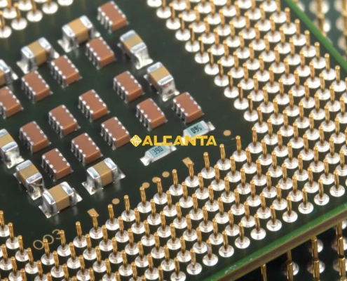
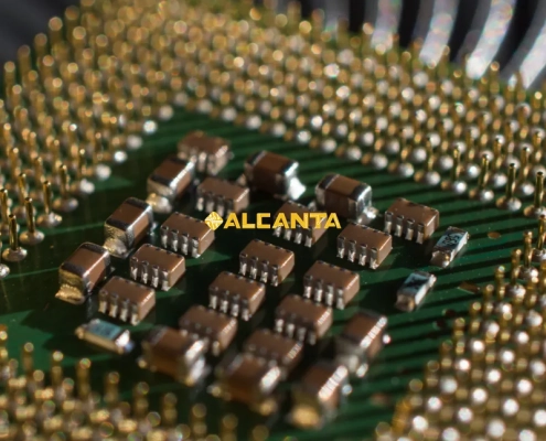
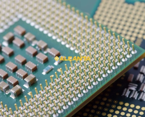
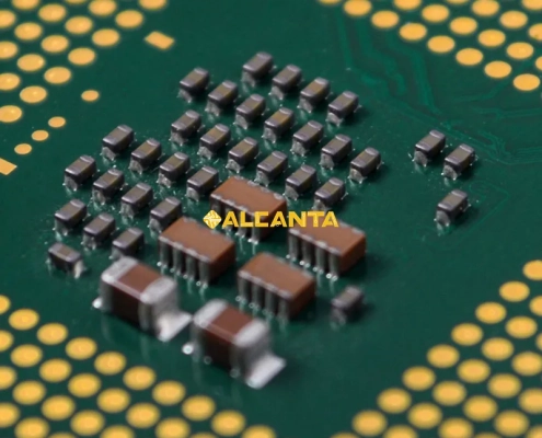
Role and Significance: The chip package substrate serves as the foundation, providing structural support and acting as a conduit for electrical connections. Its significance lies in offering a stable platform for the delicate semiconductor components, safeguarding them from mechanical stress and environmental factors.
Materials Used: Common materials for chip package substrates include organic laminates and ceramics. Each material is chosen based on its thermal conductivity, electrical properties, and cost-effectiveness. The selection is crucial, as it directly influences the package’s ability to dissipate heat and maintain electrical integrity.
Connection to the Semiconductor Device: The substrate establishes a vital electrical connection between the semiconductor device and the external world. Through a network of conductive traces, the substrate facilitates the transmission of signals, power, and data, ensuring the device’s functionality within an electronic system.
Die Substrate Package
Definition and Function: The die substrate, often synonymous with the chip carrier, encapsulates the semiconductor die within the package. Its primary function is to protect the die from external influences, such as moisture and contaminants, ensuring the longevity and reliability of the semiconductor device.
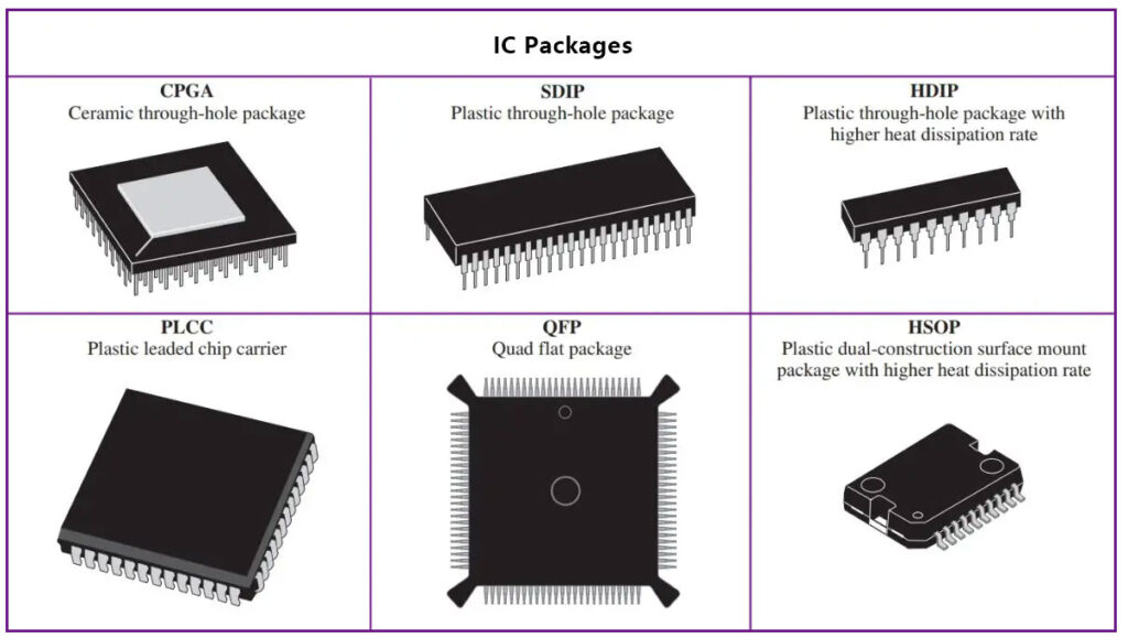
Types and Variations: Die substrates come in various forms, ranging from leaded packages like Dual In-line Packages (DIP) to surface-mounted packages like Quad Flat Packages (QFP). Each type caters to specific application requirements, addressing factors such as size constraints, thermal dissipation, and ease of assembly.
IC Packaging Materials
Materials Overview: IC packaging materials play a pivotal role in determining the overall performance and reliability of the packaged semiconductor device. Common materials include encapsulation resins, mold compounds, and lead frames. The selection involves a careful balance between mechanical strength, thermal conductivity, and electrical insulation.
Impact on Performance and Reliability: The choice of IC packaging materials directly impacts the device’s performance parameters, such as thermal dissipation, signal integrity, and resistance to environmental stress. Optimal material selection enhances the reliability of the semiconductor device, ensuring it meets stringent industry standards and end-user expectations.
Common Chip Package Types
Chip packaging plays a crucial role in ensuring the reliability, performance, and manufacturability of semiconductor devices. Below is a detailed breakdown of major chip package types, including their structures, advantages, and applications.
Flip-Chip Package
Structure of Flip-Chip
Flip-chip packaging is a high-performance method where the semiconductor die is flipped upside down and directly connected to the substrate or PCB using solder bumps instead of traditional wire bonding. The key structural elements include:
- Die (IC chip): The semiconductor component that performs the actual processing.
- Solder bumps: Tiny spheres of solder deposited onto the chip’s I/O pads, which serve as electrical and mechanical connections.
- Underfill material: A polymer material injected between the die and the substrate to enhance mechanical strength and thermal performance.
- Substrate or PCB: The board onto which the flip-chip is mounted, providing electrical routing and mechanical support.
Advantages of Flip-Chip Packaging
- Higher Performance: Shorter interconnects reduce parasitic inductance and resistance, improving signal integrity and speed.
- Better Thermal Dissipation: The direct contact between the die and the substrate allows for efficient heat transfer, making it ideal for high-power applications.
- Smaller Form Factor: Flip-chip eliminates wire bonds, enabling more compact package designs.
- Higher I/O Density: Supports a larger number of input/output connections compared to traditional wire-bonded packages.
Applications of Flip-Chip
- High-performance computing: Used in CPUs, GPUs, FPGAs, and AI accelerators.
- Mobile and consumer electronics: Found in high-end smartphones, tablets, and gaming consoles.
- Automotive and industrial electronics: Used in high-reliability applications where thermal and electrical performance is critical.
BGA (Ball Grid Array) vs. CSP (Chip Scale Package)
Ball Grid Array (BGA)
BGA is a packaging technology where the chip is mounted on a substrate, and solder balls are arranged in a grid pattern on the underside for electrical connections to the PCB.
Key Features of BGA:
- Uses solder balls instead of leaded pins, reducing mechanical stress.
- Offers higher pin density and better electrical performance than older leaded packages.
- Excellent thermal dissipation due to the direct connection between the die and PCB.
Advantages of BGA:
- Higher I/O count compared to traditional leaded packages.
- Improved electrical performance due to reduced signal interference.
- More robust mechanical structure compared to leaded packages (e.g., QFP).
Applications of BGA:
- Microprocessors and SoCs (System-on-Chip)
- Networking and communication devices
- High-performance embedded systems
Chip Scale Package (CSP)
CSP is a category of ultra-compact packages designed to be nearly the same size as the die itself, reducing overall footprint.
Key Features of CSP:
- Near die-size form factor: Typically, the package is no more than 1.2 times the die size.
- Lower profile: Ideal for space-constrained applications.
- Common types of CSP: Wafer-Level CSP (WLCSP) and Fan-In/Fan-Out CSP.
Advantages of CSP:
- Small size and lightweight, making it ideal for portable electronics.
- Simplified manufacturing process with fewer interconnect layers.
- Improved electrical performance due to shorter interconnect paths.
Applications of CSP:
- Smartphones, wearables, and compact IoT devices.
- Memory chips (e.g., Flash, DRAM).
- Sensor packages (e.g., camera modules).
Key Differences Between BGA and CSP
| Feature | BGA (Ball Grid Array) | CSP (Chip Scale Package) |
|---|---|---|
| Size | Larger than the die | Close to die size |
| I/O Count | Higher | Lower |
| Thermal Performance | Good (via PCB connection) | Moderate |
| Applications | High-performance computing, networking | Mobile devices, memory chips |
Other IC Package Types
Apart from Flip-Chip, BGA, and CSP, several other traditional and advanced IC package types are widely used in different applications.
Quad Flat Package (QFP)
- Structure: A rectangular package with gull-wing leads extending outward from all four sides.
- Advantages:
- Suitable for moderate I/O counts (up to a few hundred pins).
- Compatible with surface-mount technology (SMT).
- Cost-effective and widely used.
- Applications: Microcontrollers, low-power processors, and industrial electronics.
Quad Flat No-Lead (QFN)
- Structure: Similar to QFP but without extending leads; instead, pads are located at the bottom.
- Advantages:
- Compact and lightweight.
- Excellent thermal and electrical performance.
- Low manufacturing cost.
- Applications: Power management ICs, RF modules, sensor interfaces.
Small Outline Package (SOP)
- Structure: A rectangular, leaded package with leads extending from two sides.
- Advantages:
- Simple and low-cost.
- Compatible with automated assembly processes.
- Applications: Low-pin-count ICs such as EEPROMs, operational amplifiers, and voltage regulators.
Navigating through the intricacies of semiconductor chip packaging involves a meticulous series of steps and processes, each contributing to the integrity and functionality of the final product.
Overview of Semiconductor Chip Packaging
Step-by-Step Breakdown
- Die Attach: The semiconductor die is affixed to the package substrate using adhesive materials or solder, forming the initial connection.
- Wire Bonding: Thin wires are bonded from the semiconductor die to the package substrate, establishing electrical connections for data and power transfer.
- Encapsulation: The die and wire bonds are encapsulated within a protective material, often epoxy or molding compounds, shielding the sensitive components from external elements.
- Lead Frame Attachment: In packages with leads, the lead frame is attached, providing external connection points for the packaged device.
- Testing: Rigorous testing procedures ensure the functionality, reliability, and quality of the packaged semiconductor device.
Importance of Packaging in Final Product: The packaging process is not merely a concluding step; it profoundly influences the performance, durability, and overall functionality of the semiconductor device. Effective packaging enhances thermal management, protects against environmental factors, and facilitates integration into electronic systems.
IC Packaging Process Flow
Key Stages in IC Packaging
- Substrate Preparation: The substrate undergoes preparation, including cleaning and surface treatment, to ensure optimal conditions for die attachment.
- Die Attach and Wire Bonding: Similar to the general chip packaging process, this stage involves attaching the semiconductor die to the substrate and establishing wire bonds for electrical connections.
- Encapsulation: The die and wire bonds are encapsulated within the package material, providing mechanical support and protecting the delicate components from external influences.
- Lead Frame Integration: In leaded packages, the lead frame is integrated into the package, creating external connection points for the device.
- Testing and Quality Assurance: Thorough testing is conducted to validate the functionality and reliability of the packaged IC. This stage includes electrical testing, thermal testing, and other quality assurance measures.
Critical Processes and Techniques
- Wafer Dicing: Before packaging, semiconductor wafers are diced into individual dies, allowing for the packaging of multiple devices simultaneously.
- Flip Chip Technology: In this technique, the semiconductor die is flipped and directly bonded to the substrate, reducing the length of wire bonds and enhancing electrical performance.
- Advanced Interconnect Technologies: Utilizing technologies like Through-Silicon Vias (TSVs) and microbumps for 3D packaging, advanced interconnects improve signal integrity and enable higher data transfer rates.
Understanding the nuances of these processes is essential for ensuring the reliability and functionality of semiconductor devices, ultimately impacting the performance of the electronic systems they power.
Selecting the right chip package is a crucial decision in semiconductor design, as it directly impacts the device’s performance, thermal management, size, and manufacturing cost. Engineers must carefully evaluate various factors to ensure the package meets the specific requirements of the application. Additionally, emerging trends in chip packaging technology are reshaping the way chips are designed and integrated, influencing future package selection strategies.
Factors Influencing Package Selection
When choosing a chip package, several key factors must be considered:
Package Size and Form Factor
- Miniaturization Requirements: For applications like smartphones, wearables, and IoT devices, compact packages such as Chip-Scale Packages (CSPs) or Fan-Out Wafer-Level Packages (FO-WLPs) are preferred.
- Board Space Constraints: High-density PCBs may require smaller pitch packages such as Ball Grid Array (BGA) or Quad Flat No-Lead (QFN) to optimize routing.
- Stacking Capability: 3D chip packaging is useful when vertical stacking is necessary for memory and high-performance applications.
Performance and Electrical Considerations
- Signal Integrity: High-frequency applications, such as 5G and RF systems, benefit from Flip-Chip packaging, which reduces signal loss and improves electrical performance.
- I/O Density: Packages with higher pin counts, such as BGA and System-in-Package (SiP), enable better data throughput for advanced processors and networking chips.
- Parasitic Effects: Leaded packages (QFP, SOP) may introduce higher resistance and inductance, making them less suitable for high-speed applications.
Thermal Management and Power Dissipation
- Heat Dissipation Requirements: High-power chips, such as processors and GPUs, require packages with good thermal conductivity, like Flip-Chip BGA (FCBGA) or metal-cased packages with integrated heat spreaders.
- Cooling Solutions: Some packages, such as Power QFN (PQFN), include exposed pads to enhance heat dissipation through PCB heat sinking.
- Material Selection: Ceramic packages provide superior thermal performance but come at a higher cost.
Manufacturing and Cost Considerations
- Production Scalability: Standard lead-frame packages (e.g., QFP, SOP) are widely available and cost-effective for high-volume manufacturing.
- Assembly Complexity: Packages like FCBGA and SiP require advanced manufacturing techniques and precise substrate alignment, increasing production costs.
- Testing and Yield Impact: Wafer-level packages, such as Fan-In WLP (FI-WLP), reduce handling costs and improve yield by enabling batch testing.
Application-Specific Requirements
- Automotive Electronics: Requires high-reliability packaging, such as hermetically sealed ceramic or AEC-Q100 qualified BGA packages, to withstand extreme temperatures and vibrations.
- Consumer Electronics: Emphasizes cost efficiency and compact design, leading to the use of WLP or Molded Leadless Packages (MLPs).
- Medical Devices and Aerospace: Requires hermetic sealing and radiation-hardened packaging for long-term reliability in harsh environments.
Future Trends in Chip Packaging
As semiconductor technology advances, packaging innovation plays a crucial role in meeting the growing demands for higher performance, better thermal management, and miniaturization. Below are some of the key trends shaping the future of chip packaging technology.
3D and Heterogeneous Integration
- 3D Stacking with Through-Silicon Vias (TSVs): Enables ultra-fast data transfer by vertically integrating logic, memory, and power management chips.
- Chiplet-Based Architectures: Leading chip manufacturers are shifting towards chiplet-based designs, where different functional dies are packaged together in System-in-Package (SiP) or Advanced Multi-Chip Modules (MCMs).
- Hybrid Bonding: A new technology enabling direct copper-to-copper connections for improved performance and lower power consumption.
Fan-Out and Advanced Wafer-Level Packaging
- Fan-Out Packaging Expansion: Increasingly adopted in mobile processors, AI accelerators, and networking chips due to its high I/O capability and superior thermal performance.
- Panel-Level Packaging (PLP): A next-generation approach that uses larger substrate panels (instead of wafers) to improve production efficiency and reduce costs.
Integration of Advanced Thermal Solutions
- Embedded Cooling Structures: Future chip packaging will incorporate microfluidic cooling or embedded vapor chambers for extreme heat dissipation.
- Thermal Interface Materials (TIMs) Optimization: New high-performance TIMs will enhance heat conduction between the die and external cooling components.
AI-Optimized and Custom Packaging
- Tailored Packaging for AI and High-Performance Computing (HPC): AI processors require specialized packaging, such as CoWoS (Chip-on-Wafer-on-Substrate) or InFO (Integrated Fan-Out), to meet extreme data bandwidth and power requirements.
- Custom Packaging for Emerging Markets: Personalized packaging solutions will emerge for quantum computing, edge AI, and 5G mmWave applications.
Sustainable and Lead-Free Packaging
- Eco-Friendly Packaging Materials: The semiconductor industry is shifting toward biodegradable substrates, lead-free soldering, and halogen-free molding compounds to reduce environmental impact.
- Recyclable and Energy-Efficient Manufacturing Processes: Efforts are being made to reduce energy consumption in chip packaging and enhance recyclability.
The relentless pursuit of innovation in chip packaging has led to the emergence of cutting-edge technologies, pushing the boundaries of what is achievable in terms of miniaturization, performance, and functionality.
Advancements in Chip Packaging
Overview of Cutting-Edge Technologies
- 3D Packaging: Utilizing multiple layers of integrated circuits stacked on top of each other, 3D packaging enhances performance and reduces footprint, allowing for increased functionality within constrained spaces.
- Fan-Out Wafer-Level Packaging (FOWLP): This technology involves redistributing the connections from the traditional perimeter of the chip to the entire surface, optimizing space and enabling more efficient heat dissipation.
- Heterogeneous Integration: Combining different types of materials and technologies on a single chip, heterogeneous integration enhances performance by integrating diverse functionalities, such as memory, logic, and sensors, in a compact package.
- Advanced Interconnect Technologies: Technologies like Through-Silicon Vias (TSVs) and microbumps improve the efficiency of signal transfer between different components within the package, contributing to faster data transmission and reduced power consumption.
Future Trends and Expectations
- More Compact Designs: The trend towards smaller form factors will continue, driven by demands for portable devices and advancements in IoT. Advanced packaging will play a crucial role in achieving these compact designs.
- Increased Integration: Future chip packaging is expected to facilitate even higher levels of integration, incorporating a broader range of functionalities on a single chip. This trend aligns with the growing complexity of electronic systems.
- Enhanced Thermal Management: As electronic devices become more powerful, managing heat dissipation becomes critical. Future chip packaging is anticipated to introduce innovative thermal management solutions to address this challenge.
- Eco-Friendly Materials: With a growing emphasis on sustainability, the use of eco-friendly materials in chip packaging is expected to rise. This includes exploring recyclable and biodegradable packaging materials.
- Integration of Emerging Technologies: Advanced packaging will likely integrate emerging technologies such as photonics, neuromorphic computing, and quantum computing, paving the way for novel applications and enhanced computing capabilities.
The future of chip packaging holds exciting possibilities as the industry continues to innovate and respond to the evolving needs of technology. These advancements are poised to redefine the landscape of electronics, shaping a future where devices are not only smaller and more powerful but also more environmentally sustainable and capable of supporting groundbreaking applications.
Chip Scale Package (CSP) vs. Ball Grid Array (BGA)
Flip-Chip Package: Both CSP and BGA can use flip-chip bonding, where the die is flipped and directly connected using solder bumps. This improves electrical performance and heat dissipation, but flip-chip techniques are more common in high-performance BGA applications.
Key Differences: CSP is nearly the same size as the die, making it ideal for compact devices like smartphones and IoT sensors. It has lower I/O density and moderate thermal performance but is cost-effective. BGA, on the other hand, supports higher pin counts, offers better electrical and thermal performance, and is widely used in processors, GPUs, and networking equipment. However, BGA requires more PCB space and has higher manufacturing complexity.
Other IC Packages: In addition to CSP and BGA, packages like QFP, QFN, and SOP are used for applications requiring lower cost, simpler assembly, or different thermal characteristics.
Choosing the Right Package: CSP is best for space-constrained, low-to-moderate I/O applications, while BGA is suited for high-performance computing and high-density connections. Thermal management, cost, and reworkability are key factors in package selection.
Future Trends: Advanced packaging technologies like fan-out wafer-level packaging (FO-WLP), 3D chip stacking, and system-in-package (SiP) are evolving to enhance performance while reducing size constraints.
FAQs about Chip Packaging
What is a chip package?
A chip package is a protective enclosure that houses a semiconductor device, such as a microchip or integrated circuit (IC). It shields the delicate components from external influences and provides electrical connections for integration into electronic systems.
What is advanced chip packaging?
Advanced chip packaging refers to innovative and sophisticated techniques used in enclosing and connecting semiconductor devices. It goes beyond traditional methods, incorporating technologies like 3D stacking, fan-out packaging, and heterogeneous integration to enhance performance, miniaturization, and functionality.
What is IC packaging?
IC packaging, or Integrated Circuit packaging, is the process of enclosing a semiconductor device, often a microchip or integrated circuit, within a protective housing. This packaging ensures the device’s protection, facilitates electrical connections, and allows integration into electronic systems.
What is the process of semiconductor chip packaging?
The process of semiconductor chip packaging involves several key steps:
- Die Attach: Affixing the semiconductor die to a substrate.
- Wire Bonding: Establishing electrical connections with thin wires.
- Encapsulation: Protecting the die and wires with a protective material.
- Lead Frame Attachment: Adding external connection points if applicable.
- Testing: Rigorous testing for functionality and reliability.
- Final Assembly: Preparing the packaged chip for integration into electronic systems.

