
Navigating the Realm of Chip Carriers
In the dynamic landscape of the integrated circuit (IC) industry, chip carriers stand as indispensable components, serving as the bridge between the semiconductor chip and the broader electronic system. These carriers, in their various forms and configurations, play a pivotal role in enabling the functionality and performance of electronic devices we rely on daily. They facilitate the seamless integration of semiconductor chips into complex electronic systems, ensuring efficient signal transmission, thermal management, and mechanical support. As the demand for smaller, faster, and more powerful electronic devices continues to surge, the significance of chip carriers in enabling advancements in IC design and manufacturing cannot be overstated. From consumer electronics to industrial applications, chip carriers form the backbone of modern electronic systems, driving innovation and pushing the boundaries of what’s possible in the realm of semiconductor technology.
Fundamentals of Chip Carriers
What is a Chip Carrier?
A chip carrier, in the realm of integrated circuits (ICs), serves as a package or housing for semiconductor chips. It provides a protective and supportive enclosure for the delicate silicon die, shielding it from external contaminants, mechanical stresses, and environmental factors. Chip carriers come in various forms, including ceramic, plastic, and metal packages, each tailored to specific application requirements and manufacturing processes. These carriers feature an array of electrical contacts or leads that facilitate connections between the semiconductor chip and the larger electronic system, enabling the transmission of signals and power.
The Role and Function of Chip Carriers
Chip carriers play a crucial role in the integration of semiconductor chips into electronic systems. Their primary function is to provide a stable platform for mounting and interconnecting semiconductor chips within a circuit board or electronic assembly. By encapsulating the chip in a protective housing, chip carriers safeguard it from damage due to physical stress, moisture, temperature variations, and other environmental hazards. Additionally, chip carriers serve as conduits for heat dissipation, ensuring efficient thermal management to maintain optimal operating conditions for the semiconductor device.
In essence, chip carriers act as intermediaries between the semiconductor chip and the external environment, facilitating reliable electrical connections while ensuring the integrity and longevity of the integrated circuit. They enable the seamless integration of semiconductor technology into a diverse range of electronic applications, spanning from consumer electronics to automotive systems, telecommunications, aerospace, and beyond. As the backbone of modern electronic packaging, chip carriers play a vital role in advancing the capabilities and performance of electronic devices, driving innovation in the integrated circuit industry.
Different Types of Chip Carriers
Chip carriers come in various forms, each tailored to specific application requirements and manufacturing processes. Below is an overview of some common types of chip carrier packages:
Bare Die
Characteristics: Bare die chip carriers consist of only the semiconductor chip itself, without any encapsulation or packaging material. They typically feature bond pads for wire bonding or soldering directly to a substrate.
Advantages: Bare die packages offer the smallest footprint and lowest profile, making them ideal for applications with strict size and weight constraints. They also provide excellent thermal performance due to direct contact with the substrate.
Disadvantages: Lack of protection makes bare die vulnerable to physical damage and environmental factors. They require specialized handling during assembly and may have limited reliability compared to packaged devices.
Suitable Applications: Bare die chip carriers are commonly used in high-density applications such as microelectronics, MEMS (Microelectromechanical Systems), and sensors.
LCC (Plastic Leaded Chip Carrier)
Characteristics: PLCCs are plastic encapsulated chip carriers with leads extending from all four sides. They feature a square or rectangular shape with leads arranged along the perimeter.
Advantages: PLCC packages offer good mechanical protection, ease of handling, and compatibility with standard surface mount assembly processes. They provide reliable electrical connections and are suitable for moderate to high pin count devices.
Disadvantages: Limited thermal dissipation compared to other package types. PLCCs may also have higher inductance and lead inductance, affecting high-frequency performance.
Suitable Applications: PLCCs are commonly used in consumer electronics, automotive applications, and industrial control systems.
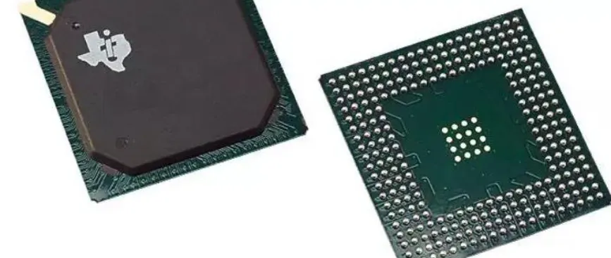
BGA (Ball Grid Array)
Characteristics: BGA chip carriers feature an array of solder balls or bumps arranged in a grid pattern on the bottom surface of the package. These solder balls serve as electrical connections to the circuit board.
Advantages: BGAs offer superior thermal and electrical performance due to reduced lead lengths and enhanced heat dissipation capabilities. They also provide excellent reliability and are less prone to solder joint failures compared to traditional leaded packages.
Disadvantages: BGA assembly requires specialized equipment and techniques, increasing manufacturing costs. Repair and rework of BGA devices are challenging due to the hidden solder connections beneath the package.
Suitable Applications: BGAs are widely used in high-performance computing, networking equipment, telecommunications, and portable devices where compact size and high reliability are critical.
Each type of chip carrier package has its unique characteristics, advantages, and disadvantages, making them suitable for specific applications based on performance, reliability, and cost considerations. Understanding the differences between these packages is crucial for selecting the most appropriate solution for a given application.
Ceramic Leaded Chip Carrier
Ceramic Leaded Chip Carriers (CLCCs) are a type of chip carrier package known for their durability, reliability, and thermal performance. They are constructed using a ceramic material for the body of the package, providing excellent mechanical strength and thermal conductivity.
Characteristics and Structure
CLCCs typically feature a ceramic substrate with metal leads extending from the sides of the package. The semiconductor chip is mounted onto the ceramic substrate and connected to the leads using wire bonding or flip-chip technology. The ceramic material used in CLCCs offers high resistance to temperature extremes, moisture, and chemical corrosion, making it suitable for harsh operating environments.
Advantages
1. Mechanical Strength: Ceramic materials provide superior mechanical strength compared to plastic packages, offering enhanced protection against physical damage and mechanical stresses.
2. Thermal Conductivity: Ceramic substrates have high thermal conductivity, allowing for efficient dissipation of heat generated by the semiconductor chip. This helps in maintaining optimal operating temperatures and improving overall device reliability.
3. Hermetic Seal: CLCCs can be hermetically sealed, providing a barrier against moisture, dust, and other contaminants. This ensures long-term reliability and stability of the enclosed semiconductor device.
4. Compatibility: CLCCs are compatible with standard surface mount assembly processes, making them easy to integrate into existing manufacturing workflows.
Application Areas
1. Military and Aerospace: CLCCs are commonly used in military and aerospace applications where reliability and ruggedness are paramount. They withstand extreme temperature fluctuations, vibration, and mechanical shock, making them ideal for harsh operating conditions.
2. Medical Devices: CLCCs find applications in medical devices where reliability and long-term performance are critical. They offer protection against sterilization processes and chemical exposure commonly encountered in medical environments.
3. Industrial Equipment: CLCCs are employed in industrial control systems, power electronics, and other industrial equipment requiring high reliability and durability. Their robust construction ensures stable performance in demanding industrial environments.
In summary, Ceramic Leaded Chip Carriers offer several advantages over other types of chip carrier packages, including superior mechanical strength, thermal conductivity, and reliability. They find applications in a wide range of industries where ruggedness, longevity, and thermal performance are essential considerations.
Cost of Chip Carriers
The cost of chip carriers is influenced by various factors, including manufacturing processes, materials used, package complexity, and market demand. Understanding these factors is crucial for assessing the overall cost-effectiveness of different chip carrier options.
Factors Influencing Cost
1. Materials: The choice of materials for the chip carrier package significantly impacts its cost. For example, ceramic and metal packages tend to be more expensive than plastic packages due to the higher cost of raw materials and manufacturing processes.
2. Package Complexity: The complexity of the chip carrier design, including the number of leads, the presence of heat sinks, and the level of integration, can affect manufacturing costs. More complex designs often require additional processing steps and specialized equipment, leading to higher production costs.
3. Assembly Processes: The assembly processes required for chip carriers, such as wire bonding, flip-chip bonding, and encapsulation, contribute to the overall cost. Automated assembly processes may incur higher upfront equipment costs but can result in lower labor costs and higher production efficiency.
4. Volume: Economies of scale play a significant role in chip carrier cost. Higher production volumes typically lead to lower per-unit manufacturing costs due to spreading fixed costs over a larger number of units.
5. Technology Node: Advancements in semiconductor manufacturing technology can influence chip carrier costs. Shrinking feature sizes and increasing integration levels may reduce the size and complexity of chip carriers, potentially lowering costs.
Relationship with Other Key Factors
1. Performance: There is often a trade-off between chip carrier cost and performance. Higher-performance chip carriers, such as those with advanced thermal management features or enhanced electrical properties, may command a higher price due to the added value they provide.
2. Reliability: Chip carriers designed for high reliability and longevity may incorporate additional features or use more robust materials, leading to higher costs. However, the cost of potential failures or downtime due to unreliable chip carriers must also be considered when evaluating overall cost-effectiveness.
3. Market Demand: Supply and demand dynamics in the chip carrier market can impact pricing. High demand for certain types of chip carriers or shortages of key materials may drive prices up, while oversupply or decreased demand may lead to lower prices.
In conclusion, the cost of chip carriers is influenced by a combination of factors including materials, package complexity, assembly processes, production volume, technology node, performance requirements, reliability considerations, and market dynamics. Balancing these factors is essential for optimizing chip carrier cost while meeting performance, reliability, and market requirements.
Future Trends of Chip Carriers
The integrated circuit industry is continuously evolving, driven by technological advancements, changing market demands, and emerging applications. The development trends of chip carriers reflect this dynamic landscape, with several key areas of innovation and improvement shaping the future of chip carrier technologies.
Analysis of Development Trends
1. Miniaturization: One prominent trend in chip carrier development is the ongoing push towards miniaturization. As electronic devices become smaller and more compact, there is a growing demand for chip carriers with reduced footprint and profile. This trend is driving innovations in packaging technologies such as wafer-level packaging (WLP), fan-out wafer-level packaging (FOWLP), and chip-scale packaging (CSP), enabling higher levels of integration and functionality in smaller form factors.
2. High-Speed Interconnects: With the increasing demand for high-speed data transmission in applications such as 5G communication, artificial intelligence, and autonomous vehicles, there is a need for chip carriers capable of supporting higher data rates and bandwidths. Future chip carriers are expected to incorporate advanced interconnect technologies such as microbumps, through-silicon vias (TSVs), and multilayer substrates to enable faster and more efficient signal transmission.
3. Enhanced Thermal Management: As semiconductor devices continue to pack more functionality into smaller packages, thermal management becomes a critical consideration. Future chip carriers are likely to feature advanced thermal management solutions such as embedded heat spreaders, thermal vias, and liquid cooling technologies to dissipate heat more effectively and ensure optimal operating temperatures for the enclosed semiconductor chips.
Prospects and Predictions
1. Integration of Heterogeneous Components: Future chip carriers are expected to facilitate the integration of heterogeneous components such as CPUs, GPUs, memory, and sensors into a single package. This trend towards system-on-chip (SoC) and system-in-package (SiP) integration enables higher levels of functionality, performance, and energy efficiency in a smaller footprint, catering to the demands of diverse applications ranging from mobile devices to Internet-of-Things (IoT) devices.
2. Advancements in Material Science: Continued advancements in material science are expected to drive innovations in chip carrier materials, enabling properties such as improved mechanical strength, thermal conductivity, and electrical performance. Novel materials such as advanced polymers, nanocomposites, and 2D materials hold promise for enhancing the performance and reliability of future chip carriers.
3. Emergence of 3D Packaging Technologies: Three-dimensional (3D) packaging technologies, such as stacked die, through-silicon vias (TSVs), and interposer-based packaging, are poised to play a significant role in the future of chip carriers. These technologies enable vertical integration of multiple semiconductor dies, increasing packaging density, reducing interconnect lengths, and improving overall system performance.
In summary, the future of chip carriers is characterized by trends towards miniaturization, high-speed interconnects, enhanced thermal management, integration of heterogeneous components, advancements in material science, and the emergence of 3D packaging technologies. These developments are expected to drive innovation and enable new capabilities in the integrated circuit industry, catering to the evolving needs of diverse applications and driving the next wave of technological advancement.
FAQs about chip carrier
A chip carrier is a type of package or housing for semiconductor chips, providing protection and electrical connections for the chip within an electronic device.
There are various types of chip carrier packages, including bare die, PLCC (Plastic Leaded Chip Carrier), BGA (Ball Grid Array), QFN (Quad Flat No-Lead), and ceramic leaded chip carrier, among others. Each type has its own characteristics, advantages, and suitable applications.
A ceramic leaded chip carrier (CLCC) is a type of chip carrier package that features a ceramic substrate with metal leads extending from the sides of the package. CLCCs offer advantages such as superior mechanical strength, thermal conductivity, and reliability compared to plastic packages.
The cost of chip carriers depends on factors such as materials used, package complexity, assembly processes, production volume, technology node, performance requirements, reliability considerations, and market dynamics. Balancing these factors is essential for optimizing chip carrier cost while meeting performance, reliability, and market requirements.

