
Navigating the Future: CCL Substrates in PCBs
In the ever-evolving landscape of electronic products, CCL substrates stand as unsung heroes, powering the devices we rely on daily. As the backbone of modern technology, CCL substrates play an indispensable role in ensuring the functionality and performance of electronic gadgets. This introduction aims to shed light on the pivotal significance of CCL substrates, elucidating their fundamental concept and multifaceted functions within the realm of PCB manufacturing. By understanding the intricate interplay between CCL substrates and electronic devices, we gain insight into how these seemingly inconspicuous materials drive innovation and propel technological advancements forward.
Definition of CCL Substrates
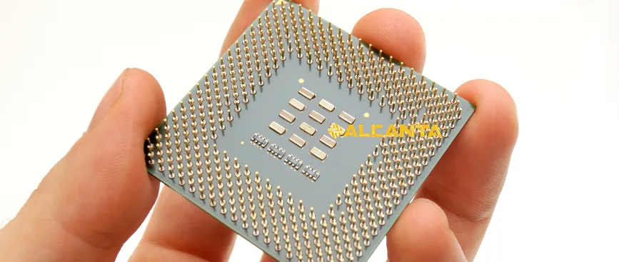
CCL substrates, or Copper Clad Laminates, serve as the foundational material in the construction of printed circuit boards (PCBs), forming the backbone upon which electronic components are mounted and interconnected. At its core, a CCL substrate consists of a thin layer of copper foil laminated onto a non-conductive substrate material, typically composed of fiberglass-reinforced epoxy resin. This lamination process creates a sturdy composite material with excellent electrical conductivity and mechanical strength, crucial for supporting the intricate network of conductive pathways found in modern electronic devices.
Basic Concept and Structure
The basic concept of CCL substrates revolves around the integration of conductive and non-conductive materials to facilitate the transmission of electrical signals while providing structural support. The structure typically comprises multiple layers, including copper foil, adhesive layers, and the substrate material. The copper foil serves as the conductive layer, while the substrate material, often referred to as the core or laminate, provides mechanical support and insulation.
Core Material in PCB Manufacturing
CCL substrates are the cornerstone of PCB manufacturing, serving as the primary material upon which the circuit pattern is etched or printed. During the manufacturing process, a layer of photoresist is applied to the copper surface of the CCL substrate, which is then exposed to UV light through a photomask, defining the desired circuit pattern. The exposed areas are then chemically etched away, leaving behind the conductive traces that define the electrical pathways of the PCB. This intricate process highlights the pivotal role of CCL substrates in shaping the functionality and performance of electronic devices, making them indispensable components in modern technology.
Composition and Characteristics of CCL Materials
CCL materials are engineered to possess specific properties that make them ideal for use in PCB manufacturing. The composition of CCL substrates typically consists of several layers, each contributing to its overall functionality and performance. The two primary components of CCL substrates are the copper foil and the substrate material, which work in tandem to provide the necessary electrical conductivity and mechanical support required for PCBs.
Copper Foil
Copper foil is the conductive layer of the CCL substrate, responsible for forming the circuit traces and providing electrical connectivity between components. The quality and thickness of the copper foil directly impact the conductivity and performance of the PCB. High-quality copper foil with uniform thickness ensures consistent electrical properties and reliable signal transmission throughout the circuit board.
Substrate Material
The substrate material, also known as the core or laminate, serves as the foundation upon which the copper foil is laminated. It is typically composed of fiberglass-reinforced epoxy resin, although other materials such as paper phenolic or polyimide may also be used depending on the application requirements. The substrate material provides mechanical support, insulation, and stability to the PCB, ensuring its structural integrity under varying operating conditions.
Conductivity, Heat Resistance, and Mechanical Properties
CCL materials exhibit excellent electrical conductivity, allowing for efficient transmission of electrical signals across the circuit board. The low electrical resistance of copper foil ensures minimal signal loss and optimal performance of electronic devices.
Moreover, CCL substrates possess high heat resistance, enabling them to withstand elevated temperatures encountered during soldering and other assembly processes. This thermal stability prevents delamination or deformation of the substrate, ensuring the reliability and longevity of the PCB.
In terms of mechanical properties, CCL materials offer robustness and durability, capable of withstanding mechanical stresses such as bending, flexing, and vibration. This mechanical resilience ensures the integrity of the PCB, even in demanding environments or under prolonged use.
Overall, the composition and characteristics of CCL materials are meticulously engineered to meet the stringent requirements of modern electronics, providing a solid foundation for the development of high-performance PCBs.
Applications of CCL Substrates
CCL substrates find extensive applications across various electronic products, playing a pivotal role in enabling the functionality and performance of modern technology. Their versatility and reliability make them indispensable components in a wide range of industries, including:
Communication Equipment
CCL substrates are extensively utilized in communication equipment such as smartphones, routers, and base stations. These devices rely on PCBs to facilitate the transmission and reception of signals, and CCL substrates provide the necessary platform for mounting and interconnecting electronic components. The high-speed data processing and connectivity demands of modern communication systems require PCBs with superior electrical performance, making CCL substrates the preferred choice for manufacturers in this sector.
Automotive Electronics
The automotive industry relies heavily on CCL substrates for various electronic components and systems, including engine control units (ECUs), infotainment systems, and advanced driver assistance systems (ADAS). CCL substrates offer exceptional durability and reliability, capable of withstanding harsh environmental conditions such as temperature fluctuations, vibrations, and moisture exposure commonly encountered in automotive applications. Their ability to support complex circuit designs and high-temperature operation makes CCL substrates essential for the continued innovation and advancement of automotive electronics.
Consumer Electronics
CCL substrates are ubiquitous in consumer electronics devices such as laptops, tablets, gaming consoles, and wearable gadgets. These devices require compact and lightweight PCBs with high-density interconnects to accommodate the growing demand for miniaturization and portability. CCL substrates provide the ideal solution, offering excellent electrical performance in a compact form factor. Additionally, their cost-effectiveness and scalability make them a preferred choice for manufacturers seeking to produce high-volume consumer electronics products.
Industrial and Aerospace Applications
In industrial and aerospace sectors, CCL substrates are utilized in a wide range of applications, including industrial control systems, aerospace instrumentation, and satellite communication systems. These applications demand PCBs with exceptional reliability, stability, and resistance to harsh operating conditions. CCL substrates excel in meeting these requirements, offering robust construction, high-temperature tolerance, and excellent electrical performance, making them indispensable for critical mission-critical applications in these industries.
Emphasizing the Crucial Role of CCL
The rapid development of electronic devices in modern technology owes much to the pivotal role played by CCL substrates. These substrates provide the essential foundation upon which electronic circuits are built, enabling the miniaturization, performance enhancement, and functionality expansion that drive innovation in the electronics industry. Without reliable and high-performance CCL substrates, the development of advanced electronic devices would be severely hindered, highlighting their crucial role in shaping the future of technology.
CCL Substrates in PCB Manufacturing
CCL substrates serve as the fundamental building blocks in the manufacturing of printed circuit boards (PCBs), playing a pivotal role in shaping the functionality and performance of electronic devices.
Foundational Material for PCBs
CCL substrates form the foundational material upon which the intricate circuitry of PCBs is constructed. The process begins with the selection of a suitable CCL substrate, which is chosen based on factors such as desired electrical properties, thermal characteristics, and mechanical strength. Once selected, the CCL substrate undergoes a series of manufacturing steps to transform it into a functional PCB.
Key Role of CCL in PCB Manufacturing
CCL substrates play a crucial role in various stages of the PCB manufacturing process, including printing, etching, and assembly:
Printing:
During the printing stage, a layer of photoresist is applied to the surface of the copper foil laminated onto the CCL substrate. The photoresist acts as a protective mask, allowing only specific areas of the copper surface to be exposed to light during the subsequent photolithography process.
Etching:
Following the printing stage, the exposed areas of the copper surface are chemically etched away, leaving behind the desired circuit traces. The CCL substrate provides the necessary support and stability during the etching process, ensuring the accuracy and precision of the circuit pattern.
Lamination:
After the circuit pattern has been defined, additional layers of substrate material and copper foil may be laminated onto the CCL substrate to create multi-layer PCBs. This lamination process involves bonding together multiple CCL substrates, each containing a layer of copper foil, to form a unified PCB with interconnected circuit layers.
Assembly:
Once the circuitry has been etched and laminated, electronic components such as resistors, capacitors, and integrated circuits are mounted onto the PCB surface. The CCL substrate provides the structural support necessary to withstand the mechanical stresses encountered during component assembly and ensures the integrity of the finished PCB.
In summary, CCL substrates play a foundational and indispensable role in the PCB manufacturing process, providing the essential platform upon which electronic circuits are constructed and facilitating the production of reliable and high-performance PCBs for a wide range of electronic applications.
Future Development of CCL Substrates
The future of CCL substrates is poised for significant advancements driven by emerging technologies and evolving industry trends. Here’s a detailed exploration of the future development trends and application prospects of CCL substrates:
Emerging Trends and Application Prospects
High-Frequency and High-Speed Applications:
As the demand for high-frequency and high-speed electronic devices continues to rise, CCL substrates will need to meet increasingly stringent performance requirements. Future developments may focus on enhancing the electrical properties of CCL substrates to support faster data transmission rates and improved signal integrity in applications such as 5G communication systems, IoT devices, and autonomous vehicles.
Flexible and Stretchable Electronics:
The growing interest in flexible and stretchable electronics presents new opportunities for CCL substrates. Future developments may involve the integration of CCL substrates with flexible or stretchable materials, enabling the production of bendable and conformable PCBs for wearable devices, medical implants, and flexible displays.
Environmentally Friendly Materials:
With increasing emphasis on sustainability and environmental responsibility, future CCL substrates may incorporate eco-friendly materials and manufacturing processes. This includes the adoption of recyclable or biodegradable substrate materials, as well as the use of alternative copper deposition methods that minimize environmental impact.
Impact of New Materials and Technologies
Nanotechnology and Advanced Materials:
The integration of nanotechnology and advanced materials holds great promise for enhancing the performance and functionality of CCL substrates. Future developments may involve the use of nanomaterials such as graphene or carbon nanotubes to improve conductivity, thermal dissipation, and mechanical strength.
Additive Manufacturing and 3D Printing:
Additive manufacturing techniques, including 3D printing, offer new avenues for the production of CCL substrates with complex geometries and tailored properties. Future advancements in additive manufacturing technologies may enable the rapid prototyping and customization of CCL substrates for specific applications, reducing lead times and production costs.
Internet of Things (IoT) Integration:
As the IoT ecosystem continues to expand, CCL substrates will play a vital role in enabling the connectivity and functionality of IoT devices. Future developments may focus on integrating CCL substrates with IoT-enabled sensors, actuators, and communication modules to create smart and interconnected systems for various industries, including healthcare, agriculture, and smart cities.
In conclusion, the future development of CCL substrates holds immense potential for revolutionizing the electronics industry, with advancements driven by emerging technologies, evolving market demands, and a growing emphasis on sustainability and innovation. As researchers and manufacturers continue to push the boundaries of materials science and engineering, CCL substrates are poised to remain at the forefront of technological innovation, shaping the way we interact with and utilize electronic devices in the years to come.
FAQs about ccl substrate
CCL stands for Copper Clad Laminate. It refers to a type of material used in the manufacturing of printed circuit boards (PCBs). CCL material consists of a thin layer of copper foil laminated onto a non-conductive substrate material, typically composed of fiberglass-reinforced epoxy resin.
A circuit board substrate is the base material upon which electronic circuits are constructed. It serves as the foundation for mounting and interconnecting electronic components. Typically made of materials like fiberglass-reinforced epoxy resin, the substrate provides mechanical support and insulation for the conductive traces and components mounted on the PCB.
Copper clad laminate (CCL) is used as the core material in the manufacturing of printed circuit boards (PCBs). It provides the surface for etching or printing the conductive pathways that form the circuitry of the PCB. CCLs offer excellent electrical conductivity and mechanical strength, making them essential for constructing reliable and high-performance electronic devices.
In a PCB, copper clad refers to the copper foil layer laminated onto the substrate material. This copper foil acts as the conductive layer of the PCB, forming the circuit traces and providing electrical connectivity between components. The copper clad is essential for creating the conductive pathways that define the functionality of the PCB.

