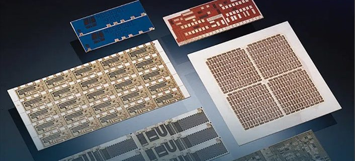
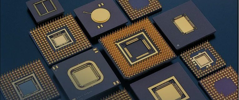
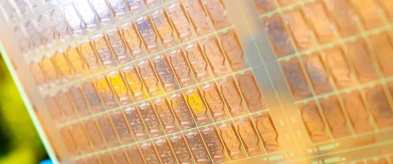
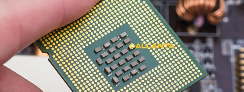
Wi-Fi technology has become an indispensable aspect of modern life, permeating homes, businesses, and public spaces worldwide. Its convenience and flexibility have revolutionized how we connect and communicate. At the heart of this wireless revolution are Wi-Fi chipsets, the unsung heroes powering our devices’ connectivity. These compact yet powerful components play a pivotal role in ensuring seamless wireless communication, enabling everything from streaming high-definition content to conducting virtual meetings. As the demand for faster speeds, greater bandwidth, and more reliable connections continues to soar, the importance of Wi-Fi chipsets only grows. Understanding their role and significance is essential in appreciating the intricate workings behind the ubiquitous Wi-Fi networks we rely on daily.
阅读更多Welcome to our blog dedicated to exploring the fundamental aspects and significance of Chip PCB products. In this comprehensive discussion, we delve into the core concepts surrounding these integral components of modern electronics. Our aim is to elucidate the critical role that Chip PCB products play in various industries and applications, from consumer electronics to aerospace engineering. Throughout this exploration, we will examine key topics such as the basics of Printed Circuit Boards (PCBs), the function and types of chips, the innovative Chip on Board (COB) technology, and the intricate relationship between chips and PCBs. Join us as we unravel the complexities and unveil the potential of Chip PCB products in shaping the future of technology.
阅读更多Semiconductor packaging technologies serve as the crucial interface between integrated circuits and their application environments. These technologies encompass various methods like Flip chip, Interposer, Dual in-line package (DIP), and more, each tailored to specific needs. Among these, Leadless Chip Carrier (LCC) emerges as a notable solution characterized by its compact design and versatile applications. LCC facilitates the secure mounting and interconnection of semiconductor chips onto circuit boards, offering a balance of performance, size, and cost-effectiveness. This introduction sets the stage to delve deeper into the realm of LCC packaging and its significance in modern electronics.
阅读更多LGA (Land Grid Array) processor packaging has revolutionized the way processors are mounted on motherboards. Unlike traditional methods like PGA (Pin Grid Array), LGA processors feature an array of pads on the processor that make direct contact with corresponding pins on the motherboard socket. This innovation not only simplifies the manufacturing process but also enhances thermal conductivity and electrical connectivity. The history of LGA packaging traces back to the early 2000s, with Intel leading the way in its adoption. Today, LGA packaging has become the standard in modern computing systems due to its numerous advantages. In this blog, we delve into the benefits of LGA processor packaging, exploring how it improves heat dissipation, simplifies installation, and enhances overall reliability.
阅读更多LGA (Land Grid Array) packaging is a crucial component in the electronics industry, facilitating the assembly and functioning of various electronic devices. Its significance lies in providing a reliable interface between integrated circuits and circuit boards, ensuring efficient electrical connections. LGA packaging finds extensive applications in consumer electronics, telecommunications, automotive, and industrial sectors due to its compact size, high performance, and thermal efficiency. The purpose of this introduction is to delve into the characteristics, advantages, and comparative analysis of LGA packaging against other packaging types such as BGA (Ball Grid Array) and QFN (Quad Flat No-Lead), shedding light on its unique features and suitability for diverse electronic applications.
阅读更多In the world of advanced electronics, how chips are packaged can make or break a device’s performance. The debate of interposer vs substrate revolves around two key components that shape the functionality, speed, and efficiency of modern systems.
An interposer acts as a bridge that connects multiple chips within a single package, enabling high-speed data transfer and efficient integration. Meanwhile, a substrate serves as the foundation, providing electrical interconnections and thermal management between the chip and the circuit board.
Understanding the unique roles of interposer vs substrate is essential to grasp how cutting-edge technologies like 2.5D packaging and high-bandwidth memory (HBM) are evolving. Both elements are pivotal in designing high-performance systems, but their differences determine when and how each should be used to achieve optimal results.
Integrated Circuit (IC) substrates play a crucial role in modern electronics, serving as the foundation for the assembly and packaging of semiconductor devices. These substrates provide a platform for mounting and interconnecting integrated circuits, enabling the creation of complex electronic systems with high functionality and performance.
In this article, we will delve into the significance of IC substrates and their application areas across various industries. Additionally, we will explore the key differences between IC substrates and Printed Circuit Boards (PCBs), discuss prominent IC substrate manufacturers, examine the composition and manufacturing processes of IC substrates, and analyze future trends shaping the evolution of IC substrate technology. Through this comprehensive overview, readers will gain a deeper understanding of the critical role that IC substrates play in advancing electronic systems and driving innovation in the semiconductor industry.
阅读更多In the realm of electronics, semiconductor packaging plays a crucial role in protecting integrated circuits (ICs) from physical damage and environmental factors, while also facilitating electrical connections. This packaging not only ensures the reliable performance of semiconductors but also enhances their compatibility with various types of electronic devices. Among the diverse packaging technologies available, Chip Scale Package (CSP) has emerged as particularly significant in modern electronics. CSP technology stands out by enabling packages that are nearly the same size as the semiconductor die they protect. This compactness is crucial for the development of smaller, more efficient, and highly integrated devices. As electronics continue to evolve towards miniaturization and higher functionality, the importance of CSP becomes increasingly pronounced, driving advancements in consumer electronics, medical devices, and automotive applications.
阅读更多Semiconductor packaging serves as the bridge between integrated circuits and the outside world, ensuring their functionality, protection, and ease of integration into electronic devices. These packages come in various forms, each tailored to specific requirements and applications. Understanding package types is crucial for engineers and designers to optimize performance, reliability, and space utilization in electronic components. Among these packaging options, the TQFP (Thin Quad Flat Package) stands out for its compactness and versatility. In this blog, we delve into the significance of semiconductor packaging and highlight the importance of the TQFP package in modern electronics.
阅读更多Teflon PCBs play a pivotal role in modern electronic applications, offering unparalleled thermal stability, electrical insulation, and signal integrity. As such, choosing the right Teflon PCB manufacturer is paramount to ensuring optimal performance and reliability in electronic devices. In this article, we delve into the significance of Teflon PCBs in today’s technology landscape, emphasizing the critical need for precision and expertise in their manufacturing process. We promise to provide a comprehensive exploration of top Teflon PCB manufacturers, highlighting their capabilities, quality standards, and contributions to the industry. Whether you’re seeking high-frequency applications or demanding environments, selecting the right Teflon PCB manufacturer is key to unlocking the full potential of your electronic designs.
阅读更多CONTACT US
4th Floor, A3 Building, HuaFeng Industrial Park, GuanTian Village, BeiHuan Road, ShiYan Street, Bao An District, Shenzhen City, Guangdong Province, China
Tel:086 (0)755-8524-1496
WhatsApp: 8615014077679
Skype: Henrychinasz
📧 pcb@alcantapcb.com
CONTACT US
SHIPPING
CERTIFCATION
recent articles
- Small Outline Integrated Circuit(SOIC) in PCB Design2025-03-12 - 2:43 上午
- TSOP/LOC Lead Frame and Its Role in Semiconductor Packaging2025-03-11 - 2:38 上午
- Key Benefits of Plastic Leaded Chip Carrier (PLCC) Lead Frame2025-03-10 - 2:47 上午
- Advantages of Plastic Dual In-line Package(PDIP) Lead Frame2025-03-07 - 3:03 上午