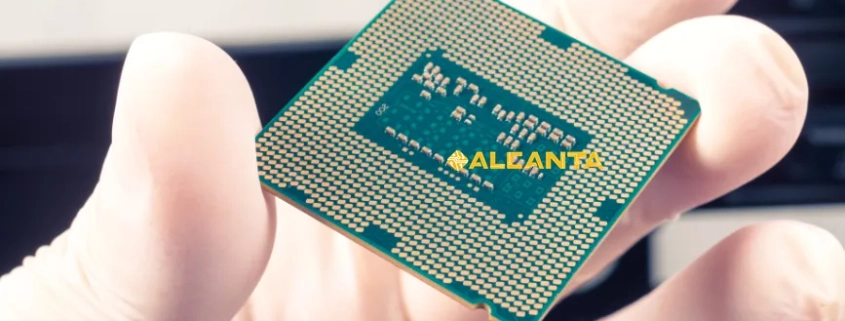
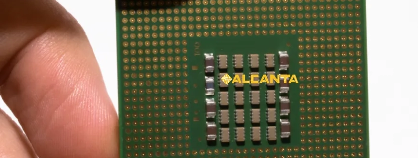
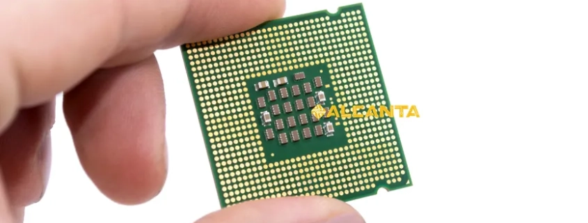
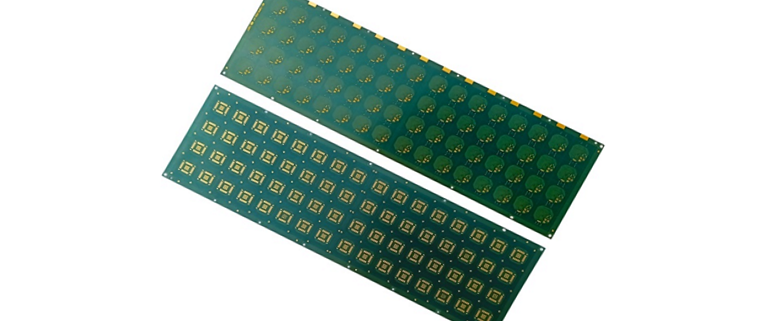
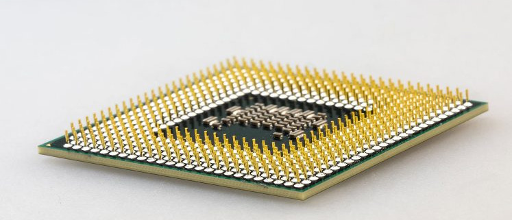
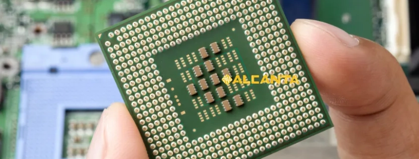
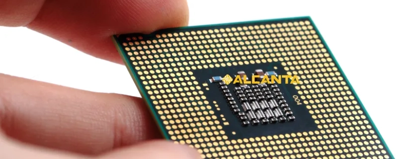
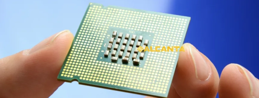
Intel Corporation stands at the forefront of the global semiconductor industry, renowned for its pioneering innovations and technological leadership. This blog aims to provide an insightful overview of Intel’s substrate products, exploring their pivotal role in the manufacturing of advanced semiconductor devices. From defining semiconductor substrates to delving into Intel’s cutting-edge chip manufacturing processes, this outline will highlight the significance of Intel’s glass substrates and TGV technology. By examining Intel’s substrate supply chain and future prospects, we aim to showcase how these components contribute to Intel’s continued dominance in shaping the future of technology.
阅读更多Intel stands at the forefront of global semiconductor manufacturing, renowned for its pioneering advancements and technological prowess. With a rich history of innovation spanning decades, Intel continues to redefine possibilities in computing and chip design. As part of its ongoing commitment to pushing the boundaries of technology, Intel introduces the Glass Core Substrate—a testament to its relentless pursuit of next-generation solutions in semiconductor packaging. This cutting-edge substrate represents a pivotal leap forward, integrating advanced materials and manufacturing techniques to enhance performance, reliability, and efficiency in IC packaging. Intel’s Glass Core Substrate not only underscores its leadership in the industry but also sets a new benchmark for future semiconductor innovations.
阅读更多Insulating substrates play a crucial role in electronic and microelectronic applications by providing electrical isolation and mechanical support for components. These substrates, including materials like HTCC, LTCC, PI, and PTFE, are essential in diverse industries due to their thermal stability and dielectric properties. Electron beam lithography (EBL) further enhances their utility by enabling precise patterning at micro- and nanoscales, crucial for manufacturing high-density electronic circuits and advanced sensors. EBL’s capability to achieve intricate patterns on insulating substrates makes it indispensable in modern semiconductor fabrication and emerging fields like microfluidics. This combination of materials and technology underscores their pivotal role in driving innovation across various electronic devices and systems.
阅读更多In the dynamic realm of electronics, Printed Circuit Boards (PCBs) are the foundation of nearly every device, from smartphones to industrial equipment. They play a vital role in providing the necessary mechanical support and electrical connections for seamless component functionality. The evolution of PCB technology has significantly enhanced performance, size, and cost efficiency, driving the miniaturization and reliability of modern electronics. This progress has also led to the development of various substrate technologies, expanding the possibilities in electronics design. A substrate in electronics serves as the base material for building electronic components and circuitry, crucially impacting the device’s performance and durability. In PCBs, materials like FR4 (fiberglass-reinforced epoxy laminate) are commonly used for their excellent support and insulation properties. Essentially, PCBs serve as the platform for mounting and interconnecting electronic components, forming the core of any electronic system. This evolution underscores the importance of substrates in advancing electronic technology.
阅读更多Substrates play a crucial role in modern technology, serving as the foundational material upon which electronic components are built and interconnected. In the realm of electronics, substrates provide the mechanical support and thermal management necessary for the reliable operation of printed circuit boards (PCBs) and integrated circuits (ICs). They ensure the precise alignment of components and facilitate efficient electrical connectivity, which is essential for the performance and miniaturization of electronic devices. In the semiconductor industry, substrates are indispensable for the fabrication of microchips, where they act as the base layer for the deposition of semiconductor materials and the formation of intricate circuit patterns. Applications of substrates span across various domains, including consumer electronics, automotive systems, telecommunications, and medical devices. Their versatility and reliability make them fundamental to advancements in technology, driving innovation and enabling the development of faster, smaller, and more efficient electronic products.
阅读更多Insulated Metal Substrates (IMS) represent a critical advancement in the realm of electronic substrates. They combine metal cores with insulating materials, offering superior thermal management and mechanical stability compared to traditional PCBs. IMS finds extensive application in high-power LED lighting, automotive electronics, and power converters where efficient heat dissipation is crucial. The growing demand for IMS stems from its ability to enhance device reliability, extend lifespan, and improve performance under demanding conditions. In today’s electronics industry, IMS plays a pivotal role in addressing thermal management challenges, thereby supporting advancements in energy efficiency and miniaturization across various electronic applications.
阅读更多Introduction to Insulated Metal Substrate (IMS) PCB begins with understanding its fundamental concept as a specialized circuit board designed for enhanced thermal management and electrical performance. IMS PCBs integrate a metal core for efficient heat dissipation, crucial for high-power applications like automotive electronics and LED lighting. In modern electronic devices, where compact size and reliability are paramount, IMS PCBs play a pivotal role due to their ability to handle thermal challenges while maintaining electrical integrity. This blog explores how IMS PCBs have become indispensable in industries requiring robust performance under demanding conditions, illustrating their significance in advancing electronic design capabilities.
阅读更多An Insulated Metal Substrate (IMS) is a specialized type of printed circuit board designed to enhance thermal management in electronic devices. It consists of a metal base layer, typically aluminum, coated with a dielectric layer to provide electrical insulation. IMS is crucial for dissipating heat efficiently from components like LEDs, power semiconductors, and automotive electronics, ensuring optimal performance and reliability. Effective thermal management not only prolongs component lifespan but also enhances overall system efficiency and safety. IMS’s ability to conduct and disperse heat makes it indispensable in modern electronics, where maintaining low operating temperatures is paramount for stable operation and performance optimization.
阅读更多Printed Circuit Boards (PCBs) are the backbone of modern electronic devices, providing the physical platform for electrical components and ensuring reliable connections through conductive pathways. They are essential in various industries, from consumer electronics to automotive and aerospace, due to their ability to enhance device performance, reduce size, and increase reliability.
As electronic devices become more compact and powerful, the demand for advanced PCB technologies has risen. Substrate-like PCB (SLP) represents a significant evolution in this field. SLPs are designed to offer higher density interconnects, improved signal integrity, and enhanced overall performance compared to traditional PCBs. This new trend in PCB technology is driven by the need for smaller, faster, and more efficient electronic devices, making SLPs a critical innovation for the future of electronics manufacturing.
阅读更多Printed Circuit Boards (PCBs) are the backbone of modern electronic devices, serving as the platform for mounting and interconnecting various electronic components. They are crucial in ensuring the functionality and reliability of everything from simple gadgets to complex machinery. PCBs provide mechanical support and establish electrical connections through conductive pathways etched from copper sheets laminated onto a non-conductive substrate. This structured layout allows for the compact and efficient design of electronic circuits, enabling the development of smaller, faster, and more powerful devices.
The purpose of this article is to delve into the concept of substrate layout within PCB design. Understanding substrate layout is essential for optimizing PCB performance, ensuring signal integrity, and enhancing overall device reliability. By exploring different types of substrates, materials used, and the significance of dielectric properties, this article aims to provide a comprehensive overview of how substrate layout influences PCB design and functionality.
阅读更多CONTACT US
4th Floor, A3 Building, HuaFeng Industrial Park, GuanTian Village, BeiHuan Road, ShiYan Street, Bao An District, Shenzhen City, Guangdong Province, China
Tel:086 (0)755-8524-1496
WhatsApp: 8615014077679
Skype: Henrychinasz
📧 pcb@alcantapcb.com
CONTACT US
SHIPPING
![]()
CERTIFCATION
![]()
recent articles
 Copper Core PCB vs Aluminium Core PCB Explained2025-09-18 - 7:13 上午
 Microwave PCB Manufacturers | RF Design and Fabrication2025-09-16 - 7:58 上午
 Flex PCB Manufacturing Process: Step-by-Step Guide2025-09-10 - 6:59 上午
 PCB Lamination Process & Sequential Lamination2025-09-04 - 8:10 上午

