
Essential PCB Design Rules for High Frequency in Electronics
With the rapid advancement of modern electronics, the demand for high-speed, high-frequency PCBs has grown significantly. Devices in industries such as 5G telecommunications, aerospace, radar systems, automotive electronics, and RF communication rely heavily on reliable signal transmission and minimal electromagnetic interference. As a result, engineers must now pay close attention to pcb design rules for high frequency to ensure performance, stability, and compliance.
While high-speed and high-frequency PCBs often overlap in application and design approaches, they are not identical. High-speed PCBs typically focus on fast data transmission rates, while high-frequency PCBs are more concerned with the signal’s operating frequency, especially in the RF and microwave ranges. Nonetheless, both require strict layout considerations, controlled impedance, and careful material selection. Understanding the fundamental differences—and the shared design challenges—is key to creating robust and reliable products that meet today’s performance standards.
Core Challenges Addressed by PCB Design Rules for High Frequency
Designing high-frequency PCBs comes with several technical challenges that, if not properly addressed, can compromise the performance of the entire system. Strict adherence to pcb design rules for high frequency is essential to ensure reliable signal transmission and electromagnetic compatibility.
One of the most critical concerns is signal integrity (SI). At high frequencies, even small discontinuities in trace layout or layer transitions can cause reflections, ringing, and timing errors. Proper trace routing, impedance matching, and return path planning are vital.
Electromagnetic interference (EMI) and crosstalk also increase with frequency. Uncontrolled energy radiation from traces can affect nearby components or signals, leading to functional failure. pcb design rules for high frequency recommend techniques such as via stitching, controlled trace spacing, and shielding to mitigate these risks.
Another major challenge is impedance control. As signals behave like transmission lines at high frequencies, trace width, dielectric thickness, and PCB material properties significantly impact signal quality.
Material selection plays a critical role. Standard FR-4 materials exhibit high loss at GHz frequencies. Designers must choose low-loss substrates like Rogers or Teflon to meet the pcb design rules for high frequency and ensure optimal electrical performance.
Key Design Guidelines in PCB Design Rules for High Frequency
To ensure optimal performance and reliability, engineers must follow specific pcb design rules for high frequency. These guidelines address the physical and electrical constraints that come into play when dealing with GHz-level signals and fast edge rates. Below are the key design principles every high-frequency PCB layout should consider.
Proper PCB Stack-up Planning in PCB Design Rules for High Frequency
A well-structured layer stack-up is foundational to effective high-frequency design. Multilayer PCBs allow better signal referencing and shorter return paths, both critical to minimizing EMI. According to pcb design rules for high frequency, placing ground and power planes close to signal layers ensures stable impedance and reduces noise coupling. Symmetrical stack-ups are also recommended to prevent board warpage during manufacturing and thermal cycling.
Controlled Impedance Design in PCB Design Rules for High Frequency
At high frequencies, transmission line effects dominate, making impedance control essential. Impedance is influenced by trace width, dielectric height, copper thickness, and the substrate’s dielectric constant (Dk). Precise impedance matching reduces signal reflections and maintains integrity. Using impedance calculators and signal integrity simulation tools during the layout phase helps predict and optimize performance.
High-Speed Layout Best Practices
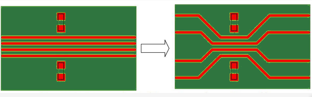
Efficient trace routing directly impacts high-frequency behavior. Routing should be as short and direct as possible, with minimal stubs or sharp angles. 90° trace corners can cause signal reflections and should be replaced with 45° bends or smooth arcs. For differential pairs, match trace lengths and spacing to maintain consistent impedance. Minimizing vias is another essential tip in pcb design rules for high frequency, though when necessary, stitching vias should be used to maintain solid return paths.
Ground and Power Plane Design
Solid ground planes are vital for high-frequency return paths and signal referencing. Discontinuities in ground can lead to impedance breaks and EMI issues. The pcb design rules for high frequency emphasize the importance of reducing ground loop areas and maintaining a continuous plane beneath signal traces. Decoupling capacitors should be placed close to power pins to filter noise and stabilize voltage levels.
EMI/EMC Control Techniques
Controlling electromagnetic interference is one of the top priorities in high-frequency PCB design. Via stitching around sensitive zones or along the board edge can help contain radiation. Shielding critical components and isolating analog and digital domains are recommended practices. Furthermore, keeping high-frequency traces away from board edges reduces unintended emissions.
Key Rules to Follow in PCB Design Rules for High Frequency
To effectively manage electromagnetic performance and signal integrity, designers must apply specific layout rules that are foundational to pcb design rules for high frequency. These rules help control crosstalk, reduce electromagnetic radiation, and ensure a stable operating environment for high-speed signals.
The 20H Rule
A critical principle in high-frequency PCB design, the 20H Rule is used to minimize power plane radiation. This rule recommends that the power plane be inset from the ground plane edge by a distance equal to 20 times the dielectric thickness (H) between them. The idea is that this offset causes the fringing electric field at the edge of the power plane to cancel out, thereby reducing EMI emissions.
Practical Example:
If the dielectric between the power and ground planes is 0.25 mm, then the power plane should be shrunk inward by 5 mm (20 × 0.25 mm) relative to the ground plane. This technique is especially effective in multilayer boards used in RF, aerospace, or automotive designs where EMI compliance is critical.
The 3W & 3H Rules
Both the 3W and 3H Rules are vital components of pcb design rules for high frequency, aimed at reducing signal coupling and mutual interference between traces.
-
3W Rule: To minimize crosstalk, traces carrying high-frequency signals should be spaced at least three times the width of a single trace apart. This reduces the electric field overlap between adjacent traces, especially in tightly packed layouts.
-
3H Rule: To avoid vertical interference between layers, the vertical spacing between two adjacent high-frequency signal layers should be at least three times the dielectric height (H) between them. This rule helps reduce mutual inductance and capacitive coupling, which are common issues in high-density multilayer PCBs.
Use Case Example:
In high-speed communication boards (e.g., SerDes or DDR routing), applying the 3W Rule can significantly reduce near-end and far-end crosstalk, while the 3H Rule ensures vertical layer isolation in complex stack-ups.
By incorporating these rules early in the layout process, designers can meet stringent design standards for high-frequency applications and improve overall signal fidelity and system reliability.
Material Selection Guidelines in PCB Design Rules for High Frequency
Choosing the right PCB substrate material is fundamental to meeting the pcb design rules for high frequency, as material properties directly affect signal loss, impedance, and overall signal fidelity. At GHz-level frequencies, even minor dielectric inconsistencies can lead to significant performance degradation.
Limitations of Standard FR-4 at High Frequencies
While FR-4 is widely used for general-purpose PCBs, it has major limitations when applied to high-frequency applications. Its relatively high Dk (Dielectric Constant) variation and high Df (Dissipation Factor) lead to increased signal attenuation, especially above 1 GHz. These losses manifest as reduced signal amplitude, higher jitter, and potential timing errors — all of which compromise signal integrity and overall performance.
High-Performance Substrates
To overcome these challenges, it is recommended to use advanced materials specifically engineered for RF and microwave circuits. Some commonly used high-performance substrates include:
-
Rogers (e.g., RO4003, RO4350) – Known for low loss, stable Dk, and ease of processing
-
Teflon (PTFE) – Offers extremely low Df and excellent high-frequency performance, ideal for RF and aerospace systems
-
Taconic – Delivers a good balance of performance and cost with low dielectric loss and high thermal stability
These materials reduce signal degradation, improve impedance control, and maintain performance across a wide frequency range.
Choosing by Dk and Df
The Dielectric Constant (Dk) affects impedance and signal propagation speed, while the Dissipation Factor (Df) influences how much signal energy is lost as heat. In line with pcb design rules for high frequency, designers should aim for a low and stable Dk (typically between 3.0–3.5) and a low Df (below 0.005) to maintain signal clarity and minimize distortion.
By selecting the appropriate substrate based on electrical performance metrics, designers can significantly enhance signal integrity and ensure optimal performance.
The Role of Rigid-Flex PCBs in PCB Design Rules for High Frequency
Rigid-flex PCBs have become a vital design choice in modern high-frequency electronics, especially where space constraints, flexibility, and high reliability are essential. Their unique structure — combining rigid layers with flexible interconnects — enables innovative layouts that align closely with key pcb design rules for high frequency.
Enhanced Signal Integrity with Fewer Connectors
One of the primary benefits of rigid-flex PCBs in high-frequency environments is their ability to reduce the number of connectors and inter-board interfaces, which are common sources of signal degradation. Every connector introduces potential for signal reflection, loss, and EMI. By designing a unified rigid-flex layout, engineers can create continuous signal paths, significantly improving signal integrity and satisfying pcb design rules for high frequency that prioritize uninterrupted transmission.
Reduced Impedance Discontinuities
Rigid-flex architectures also minimize impedance discontinuities that often occur at the junctions of separate PCBs or flex cables. In high-frequency applications, even slight mismatches in impedance can lead to reflections and timing errors. By maintaining uniform trace geometry and material properties across both rigid and flexible sections, rigid-flex designs support controlled impedance — a core requirement of pcb design rules for high frequency.
Application Examples
Rigid-flex PCBs are increasingly found in high-demand sectors that operate at or above GHz frequencies:
-
Wearable Technology – Where compact, flexible, and high-speed performance is essential for biosensors and communication modules
-
Aerospace Systems – Where vibration resistance, EMI shielding, and compact RF routing are crucial
-
Defense Electronics – Where rugged environments require both flexibility and robust high-frequency signal handling
By integrating these design advantages, rigid-flex PCBs help meet stringent high-frequency design requirements while offering mechanical reliability and electrical precision.
PCB Assembly Considerations in PCB Design Rules for High Frequency
Successful implementation of pcb design rules for high frequency doesn’t end with layout—it extends into the assembly process. Assembly quality directly impacts the electrical performance and reliability of high-frequency PCBs, particularly as signal speeds and frequencies increase. Even minor deviations in soldering, placement, or material handling can compromise critical design goals such as impedance control and signal integrity.
Precision in Soldering and Component Placement
High-frequency designs often involve tight tolerances and miniature components like fine-pitch BGAs, microstrip components, and RF modules. Any misalignment or excess solder can introduce parasitic effects, altering impedance and causing signal reflections. Therefore, automated precision placement and reflow profiles must be carefully controlled to meet the required performance standards.
Material Handling for Specialized Substrates
Substrates like Rogers, Teflon (PTFE), and other high-frequency laminates are more sensitive to temperature, moisture absorption, and mechanical stress compared to standard FR-4. These materials may expand or delaminate under improper conditions. Following strict handling protocols—such as pre-baking, temperature-controlled storage, and ESD-safe environments—is essential to preserve the material properties that are critical for maintaining performance in high-frequency applications.
Manufacturer Communication and Tolerances
To ensure that the assembled board performs as intended, designers must maintain close communication with the PCB manufacturer and assembler. This includes sharing precise specifications for controlled impedance, stack-up structure, material choices, and dimensional tolerances. Additionally, high-frequency boards may require advanced RF testing, TDR (Time Domain Reflectometry), or vector network analysis to validate signal integrity and ensure compliance with design standards.
By integrating these assembly-focused practices into the broader design workflow, teams can ensure that the final product performs consistently in real-world high-frequency environments.

