
advanced chip packaging
Welcome to our blog, where we delve into the dynamic realm of Advanced Chip Packaging technology. In this digital age, where the demand for faster, smaller, and more powerful electronic devices continues to soar, Advanced Chip Packaging stands as a critical enabler. Through this blog, we aim to shed light on the significance and far-reaching impact of Advanced Chip Packaging in the semiconductor industry.
Structured as a comprehensive exploration, our blog will first provide an overview of Chip Packaging technology, elucidating its fundamental concepts and classifications. Subsequently, we will delve into the pivotal role Advanced Chip Packaging plays, discussing its current trends, challenges, and future prospects. Furthermore, we will delve into specific packaging technologies such as Chip Act Packaging, alongside analyzing state-of-the-art chip designs and successful case studies. Join us as we embark on a journey to uncover the transformative power of Advanced Chip Packaging.
Overview of Chip Packaging Technology
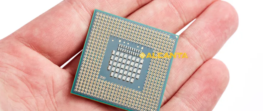
Chip packaging technology serves as a crucial link between semiconductor devices and their applications, providing protection, interconnection, and thermal management for integrated circuits (ICs). At its core, chip packaging involves encapsulating the semiconductor die within a protective casing and connecting it to external components or systems.
Concept and Function:
Chip packaging technology encompasses a range of processes and materials aimed at safeguarding the delicate semiconductor die while facilitating its integration into electronic systems. Its primary functions include:
1. Protection: Shielding the semiconductor die from environmental factors such as moisture, dust, and mechanical stress.
2. Interconnection: Establishing electrical connections between the semiconductor die and external components or systems, enabling data transmission and power distribution.
3. Thermal Management: Dissipating heat generated by the semiconductor device to prevent overheating and maintain optimal operating conditions.
Basic Principles:
Chip packaging technology operates based on several fundamental principles, including:
1. Die Attach: Affixing the semiconductor die onto a substrate or carrier using adhesives or soldering techniques.
2. Wire Bonding: Connecting the die to the substrate through fine wires made of materials like gold or aluminum.
3. Encapsulation: Sealing the die and wire bonds within a protective material such as epoxy resin or molding compound to shield them from external elements.
4. Lead Frame or Substrate Design: Providing a structural framework or substrate for mounting the semiconductor die and facilitating electrical connections.
5. Testing and Quality Assurance: Conducting rigorous testing procedures to ensure the reliability and functionality of packaged semiconductor devices.
Classification:
Chip packaging technology can be classified into several categories based on various criteria, including:
1. Package Type: Such as dual in-line package (DIP), quad flat package (QFP), ball grid array (BGA), and flip-chip package.
2. Mounting Method: Including surface-mount technology (SMT), through-hole mounting, and flip-chip bonding.
3. Material Composition: Such as ceramic, plastic, or organic substrates.
4. Interconnection Technology: Such as wire bonding, flip-chip bonding, and advanced packaging techniques like System-in-Package (SiP) and Wafer-level Packaging (WLP).
By understanding these principles and classifications, manufacturers can select the most suitable chip packaging technology to meet the specific requirements of their semiconductor devices and applications.
Significance of Advanced Chip Packaging
Advanced Chip Packaging stands as a cornerstone in the evolution of the semiconductor industry, offering a myriad of benefits and opportunities for innovation. Its significance reverberates across various facets, from enhancing chip performance to driving innovation and cost reduction.
1. Enhancing Chip Performance:
Miniaturization: Advanced Chip Packaging enables the integration of more components into smaller spaces, leading to higher component density and improved performance.
Thermal Management: Efficient thermal dissipation techniques employed in Advanced Chip Packaging mitigate heat-related issues, allowing chips to operate at higher speeds without overheating.
Electrical Performance: Advanced packaging techniques optimize signal integrity and reduce signal losses, ensuring faster data transmission and lower power consumption.
2. Reducing Costs:
Yield Improvement: Advanced packaging technologies contribute to higher manufacturing yields by reducing defects and increasing production efficiency.
Material Savings: By integrating multiple functions into a single package, Advanced Chip Packaging minimizes the need for additional components, leading to cost savings in material procurement and assembly processes.
Scalability: Advanced packaging techniques facilitate the development of scalable solutions, allowing manufacturers to adapt to varying market demands and optimize production costs.
3. Driving Innovation:
Heterogeneous Integration: Advanced Chip Packaging enables the integration of diverse components, such as processors, memory, and sensors, onto a single chip, fostering innovation in areas like IoT, AI, and autonomous systems.
System-Level Integration: By incorporating system-level functions within the chip package, Advanced Chip Packaging enables the development of compact, multifunctional devices with enhanced capabilities.
Design Flexibility: Advanced packaging techniques offer greater design flexibility, enabling engineers to explore new architectures and functionalities, thereby driving continuous innovation in semiconductor products.
In essence, Advanced Chip Packaging serves as a catalyst for progress in the semiconductor industry, unlocking new possibilities for performance optimization, cost reduction, and innovation-driven growth. Its strategic importance will only continue to grow as technological advancements and market demands evolve.
Current Trends and Challenges in Advanced Chip Packaging
Current Trends in Advanced Chip Packaging:
1. Heterogeneous Integration: There is a growing trend towards integrating diverse components, such as processors, memory, and sensors, onto a single chip, enabling more efficient and compact devices.
2. Fan-Out Wafer Level Packaging (FOWLP): FOWLP is gaining popularity due to its ability to achieve higher component density, improved electrical performance, and cost-effectiveness compared to traditional packaging methods.
3. 2.5D/3D Integration: 2.5D and 3D integration techniques enable stacking multiple dies vertically or horizontally, resulting in shorter interconnect lengths, improved performance, and reduced form factor.
4. Advanced Interconnect Technologies: Innovations in interconnect technologies, such as through-silicon vias (TSVs), microbumps, and redistribution layers (RDLs), are driving advancements in signal integrity, power delivery, and thermal management.
5. System-in-Package (SiP): SiP solutions are gaining traction for their ability to integrate multiple components, including processors, memory, and RF modules, into a single package, facilitating modular and customizable system designs.
Challenges Faced in Implementing Advanced Chip Packaging:
1. Cost: The implementation of advanced packaging technologies often requires significant investment in equipment, materials, and R&D, posing a challenge for smaller companies and startups.
2. Complexity: Advanced packaging techniques introduce complexities in design, manufacturing, and testing processes, requiring expertise and resources to overcome technical challenges and ensure product reliability.
3. Integration Challenges: Integrating diverse components onto a single chip or package demands careful coordination of design, materials selection, and manufacturing processes to ensure compatibility, reliability, and performance.
4. Reliability: With the increasing complexity of advanced packaging solutions, ensuring long-term reliability and durability becomes a critical challenge, especially in applications with stringent reliability requirements, such as automotive and aerospace.
5. Supply Chain Management: Advanced packaging technologies rely on a complex ecosystem of suppliers, equipment manufacturers, and materials providers, necessitating effective supply chain management to ensure timely delivery of components and materials.
Addressing these challenges requires collaboration across the semiconductor industry, along with ongoing innovation and investment in research and development. Overcoming these hurdles will be essential to unlocking the full potential of advanced chip packaging and realizing its benefits in driving the next wave of technological advancement.
Future Prospects of Advanced Chip Packaging
Exploring Future Development Directions:
1. Enhanced Integration: Advanced Chip Packaging will continue to evolve towards achieving higher levels of integration, enabling the integration of more diverse components onto a single chip or package. This includes further advancements in 3D integration techniques, such as through-silicon vias (TSVs) and microbumps, to enable denser and more efficient chip stacking.
2. AI and Machine Learning Integration: With the proliferation of artificial intelligence (AI) and machine learning (ML) applications, Advanced Chip Packaging will play a crucial role in enabling the integration of specialized hardware accelerators, such as neural processing units (NPUs) and tensor processing units (TPUs), into semiconductor devices for improved performance and energy efficiency.
3. Advanced Materials and Manufacturing Processes: Future advancements in materials science and manufacturing processes will drive the development of new packaging materials and techniques with enhanced thermal conductivity, electrical performance, and reliability. This includes the adoption of novel materials like advanced polymers, nanomaterials, and advanced metallization schemes.
4. Flexible and Stretchable Electronics: There is a growing demand for flexible and stretchable electronics in applications such as wearable devices, IoT sensors, and medical implants. Advanced Chip Packaging will play a key role in enabling the integration of semiconductor components onto flexible substrates, allowing for the development of conformable and stretchable electronic systems.
Analyzing Application Prospects:
1. 5G and IoT: Advanced Chip Packaging will enable the development of compact and energy-efficient devices for 5G communication infrastructure and IoT applications. This includes the integration of RF front-end modules, power management circuits, and sensor arrays onto a single chip or package.
2. Autonomous Vehicles: Advanced Chip Packaging will be essential for the development of high-performance computing platforms for autonomous vehicles, enabling the integration of sensors, processors, and memory modules into compact and ruggedized packages capable of withstanding harsh automotive environments.
3. Healthcare and Biomedical Devices: Advanced Chip Packaging will facilitate the development of advanced medical devices and diagnostic tools, including implantable sensors, smart wearables, and point-of-care diagnostic systems. This includes the integration of bio-compatible materials and miniaturized electronics for improved patient monitoring and healthcare delivery.
4. Edge Computing and AI: With the proliferation of edge computing and AI applications, Advanced Chip Packaging will enable the development of compact and energy-efficient computing
Chip Act Packaging Technology
Introducing the Features and Advantages:
Chip Act Packaging (CAP) technology represents a significant advancement in semiconductor packaging, offering several distinctive features and advantages:
1. Miniaturization: CAP enables the integration of active components, such as transistors and sensors, directly onto the package substrate, resulting in a more compact and space-efficient design compared to traditional packaging methods.
2. High Performance: By integrating active components closer to the chip, CAP minimizes signal propagation delays and reduces interconnect lengths, resulting in improved electrical performance and reduced power consumption.
3. Enhanced Functionality: CAP allows for the integration of additional functionalities, such as signal conditioning, amplification, and sensing, directly onto the package substrate, enabling the development of highly integrated and multifunctional semiconductor devices.
4. Cost Efficiency: CAP reduces the need for additional discrete components and simplifies the assembly process, leading to cost savings in material procurement, manufacturing, and assembly.
5. Reliability: CAP technology improves the reliability of semiconductor devices by reducing the number of interconnects and solder joints, thereby minimizing the risk of electrical failures and improving long-term device performance.
Analyzing the Impact on the Semiconductor Industry:
1. Innovation Catalyst: CAP technology serves as a catalyst for innovation in the semiconductor industry by enabling the development of highly integrated and multifunctional semiconductor devices. It allows designers to explore new architectures and functionalities, leading to the development of novel products and solutions.
2. Performance Enhancement: CAP technology enhances the performance of semiconductor devices by reducing signal propagation delays and improving electrical performance. This is particularly beneficial for high-speed and high-frequency applications, such as data centers, telecommunications, and automotive electronics.
3. Cost Reduction: CAP technology offers cost-saving opportunities for semiconductor manufacturers by simplifying the assembly process and reducing the number of discrete components required. This leads to lower material costs, reduced manufacturing overheads, and improved overall cost efficiency.
4. Market Differentiation: Semiconductor manufacturers can leverage CAP technology to differentiate their products in the market by offering enhanced functionality, improved performance, and reduced form factors compared to competitors. This allows companies to target niche markets and address specific customer needs more effectively.
5. Supply Chain Optimization: CAP technology streamlines the semiconductor supply chain by reducing the number of suppliers and components required for device assembly. This simplifies logistics and inventory management, leading to improved supply chain efficiency and reduced lead times.
In conclusion, Chip Act Packaging technology represents a significant advancement in semiconductor packaging, offering a wide range of features and advantages that have transformative implications for the industry. Its ability to enable innovation, enhance performance, reduce costs, and streamline supply chains positions CAP technology as a key enabler of future semiconductor developments.
State-of-the-Art Chip Designs:
Discussing Current State-of-the-Art Chip Design Technologies:
1. System-on-Chip (SoC) Architecture: SoC architecture integrates multiple functional blocks, such as processors, memory, and I/O interfaces, onto a single chip, enabling compact and highly integrated semiconductor devices. Advanced SoC designs leverage techniques such as heterogeneous integration, 3D stacking, and advanced process nodes to optimize performance, power efficiency, and form factor.
2. Multi-Core Processors: Multi-core processors incorporate multiple processing cores onto a single chip, allowing for parallel execution of tasks and improved overall performance. State-of-the-art designs utilize advanced microarchitecture techniques, such as out-of-order execution, speculative execution, and advanced cache hierarchies, to maximize throughput and efficiency.
3. Custom ASICs (Application-Specific Integrated Circuits): Custom ASICs are designed for specific applications or use cases, offering tailored performance, power, and area characteristics. Modern ASIC designs employ advanced design automation tools, hardware description languages (HDLs), and verification methodologies to streamline the design process and optimize performance.
4. FPGA (Field-Programmable Gate Array) Technology: FPGAs provide programmable logic resources that can be configured to implement custom digital circuits, enabling rapid prototyping and reconfigurability. State-of-the-art FPGA designs leverage advanced process nodes, high-speed interfaces, and sophisticated routing architectures to achieve higher performance, lower power consumption, and greater flexibility.
Analyzing Interaction with Advanced Chip Packaging:
1. Integration and Miniaturization: State-of-the-art chip design technologies often require high levels of integration and miniaturization to achieve their performance goals. Advanced Chip Packaging techniques, such as 3D stacking and heterogeneous integration, complement these design requirements by enabling the integration of multiple components onto a single package, reducing interconnect lengths, and improving signal integrity.
2. Performance Optimization: Advanced Chip Packaging plays a crucial role in optimizing the performance of state-of-the-art chip designs by providing efficient thermal management, reducing signal propagation delays, and enabling higher interconnect densities. Techniques such as Fan-Out Wafer Level Packaging (FOWLP) and System-in-Package (SiP) enable designers to achieve higher levels of performance without compromising on form factor or power efficiency.
3. Power Efficiency: Advanced Chip Packaging techniques contribute to improving the power efficiency of state-of-the-art chip designs by enabling better thermal dissipation, reducing parasitic capacitance, and optimizing power delivery networks. By integrating power management circuits and sensors directly onto the package substrate, designers can achieve finer-grained control over power consumption and thermal performance.
4. Design Flexibility: Advanced Chip Packaging offers designers greater flexibility in implementing state-of-the-art chip designs by providing alternative packaging configurations, materials, and interconnect options. This flexibility allows designers to explore new architectures, optimize performance, and address specific application requirements more effectively.
In summary, the interaction between state-of-the-art chip design technologies and Advanced Chip Packaging is symbiotic, with each complementing and enhancing the capabilities of the other. By leveraging advanced packaging techniques, designers can maximize the performance, power efficiency, and flexibility of their chip designs, driving innovation and advancement in the semiconductor industry.
FAQs about advanced chip packaging
Chip packaging technology refers to the process of enclosing semiconductor chips in protective casings or packages, which provide electrical connections, mechanical support, and thermal dissipation. This packaging is essential for protecting the chip from external elements and facilitating its integration into electronic devices.
The future of advanced packaging lies in continued innovation towards achieving higher levels of integration, improved performance, and reduced form factors. This includes advancements in technologies such as 3D integration, heterogeneous integration, and advanced materials, enabling the development of more compact, efficient, and capable semiconductor devices.
The most advanced chip designs often incorporate cutting-edge technologies such as FinFET transistors, 3D stacking, and advanced interconnects. These designs leverage the latest process nodes and microarchitecture techniques to achieve high levels of performance, energy efficiency, and integration. Examples include high-performance CPUs, GPUs, and AI accelerators used in applications such as data centers, smartphones, and autonomous vehicles.
The chip Act package (CAP) is a type of advanced chip packaging technology that integrates active components, such as transistors and sensors, directly onto the package substrate. CAP enables compact, highly integrated semiconductor devices with improved performance, reduced power consumption, and enhanced functionality. This technology represents a significant advancement in semiconductor packaging, driving innovation in various industries.


发表评论
Want to join the discussion?Feel free to contribute!