
Flip Chip Package Substrate
Flip Chip Package Substrate (FCPS) plays a pivotal role in modern integrated circuit (IC) packaging, revolutionizing the way electronic devices are assembled and enhancing their performance across various industries. In this blog, we’ll delve into the significance of FCPS and its wide-ranging application areas, spanning consumer electronics, telecommunications, automotive, and beyond. We’ll explore its evolution, distinctive features, and manufacturing processes, shedding light on how FCPS surpasses traditional packaging technologies. Moreover, we’ll compare FCPS with IC substrates and printed circuit boards (PCBs), highlighting its advantages in terms of density, performance, and cost-effectiveness. Through this comprehensive examination, readers will gain a deeper understanding of FCPS and its implications for the future of electronics packaging.
What is Flip Chip Package Substrate?
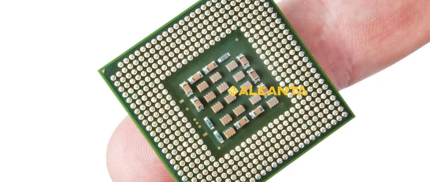
Flip Chip Package Substrate (FCPS) represents a significant advancement in integrated circuit (IC) packaging technology. At its core lies the Flip Chip method, a packaging technique where the semiconductor die is mounted face-down onto the substrate, with its active circuitry facing the substrate. This contrasts with traditional wire bonding, where the die is mounted upright and connected to the substrate via wire bonds.
FCPS enhances this Flip Chip process by providing a specialized substrate optimized for this packaging technique. The substrate serves as a foundation for mounting the semiconductor die, providing electrical connections and facilitating thermal dissipation. It is engineered with advanced materials and design features to meet the demands of modern electronics, including high-density interconnections and improved thermal management.
The role of FCPS in IC packaging is paramount. By enabling direct electrical connections between the die and the substrate without the need for wire bonds, FCPS offers several advantages. These include reduced parasitic effects, improved signal integrity, and enhanced thermal performance. Moreover, FCPS allows for higher packaging densities, enabling the development of smaller, more efficient electronic devices.
In essence, FCPS serves as a crucial component in the assembly of modern ICs, providing the necessary infrastructure for efficient and reliable device operation. Its integration into electronic systems has contributed to advancements in various fields, from consumer electronics to aerospace applications, making it a cornerstone of contemporary semiconductor packaging.
Evolution of Packaging Substrates
Traditional packaging substrate technologies have played a crucial role in the evolution of integrated circuit (IC) packaging, offering solutions for connecting semiconductor dies to the external world. Among these, Printed Circuit Boards (PCBs) and IC substrates have been widely utilized.
PCBs, the foundation of electronic devices, provide a platform for mounting and interconnecting various electronic components. They are typically composed of layers of insulating material with conductive traces etched onto them. While PCBs excel in providing connectivity for discrete components, they are limited in their ability to handle the complex requirements of IC packaging, especially with the miniaturization trend.
IC substrates emerged as a specialized solution to address the challenges of IC packaging. These substrates, often made of materials like ceramics or laminate, provide a more robust platform for mounting semiconductor dies. They offer finer pitch interconnects and improved thermal performance compared to traditional PCBs, making them suitable for high-performance applications.
However, the development of Flip Chip technology marked a significant turning point in IC packaging. Unlike wire bonding, which has been the standard method for connecting semiconductor dies to substrates, Flip Chip technology enables direct connections between the die and substrate. This approach offers numerous advantages, including shorter interconnect lengths, reduced parasitic effects, and improved signal integrity.
As Flip Chip technology gained prominence, the need for specialized substrates optimized for this packaging technique became apparent, leading to the emergence of Flip Chip Package Substrates (FCPS). FCPS combines the advantages of Flip Chip technology with advanced substrate materials and design features, paving the way for more efficient and compact IC packaging solutions.
In summary, the evolution of packaging substrates has been driven by the demand for higher performance, smaller form factors, and improved reliability in electronic devices. The development of Flip Chip technology and the subsequent introduction of FCPS represent significant milestones in this ongoing evolution, shaping the landscape of modern IC packaging.
Features of Flip Chip Package Substrate
Flip Chip Package Substrate (FCPS) offers a multitude of advantages over traditional packaging technologies, making it a preferred choice for modern integrated circuit (IC) packaging.
Higher Density and Better Thermal Performance:
FCPS enables higher packaging densities by eliminating the need for wire bonds, allowing for closer proximity of semiconductor dies. This results in more compact designs, reducing the overall footprint of electronic devices. Additionally, FCPS utilizes advanced substrate materials and design techniques to enhance thermal performance. These substrates offer improved heat dissipation capabilities, ensuring optimal operating temperatures for ICs even in high-power applications.
Importance in High-Frequency and High-Speed Applications:
FCPS is particularly well-suited for high-frequency and high-speed applications, where signal integrity is critical. The direct connection between the die and substrate minimizes parasitic effects, such as inductance and capacitance, associated with traditional wire bonding methods. This reduction in parasitics translates to improved signal integrity, enabling higher data rates and better performance in applications such as telecommunications, data centers, and high-performance computing.
Improvement in Signal Integrity:
With FCPS, signal paths are shortened, leading to reduced signal propagation delays and attenuation. This results in cleaner and more reliable signal transmission, enhancing the overall performance of electronic systems. Moreover, FCPS allows for finer pitch interconnections, enabling tighter coupling between the die and the substrate. This tight coupling reduces signal reflections and crosstalk, further improving signal integrity in high-speed digital and analog circuits.
In summary, FCPS offers a combination of benefits that address the evolving demands of modern electronics. Its ability to achieve higher packaging densities, better thermal performance, and improved signal integrity makes it an indispensable component in high-performance electronic devices, driving innovation across various industries.
Composition and Manufacturing Process of FCPS
Components of FCPS:
Flip Chip Package Substrate (FCPS) comprises several key components carefully engineered to meet the demands of modern integrated circuit (IC) packaging.
1. Substrate Materials: FCPS substrates are typically made from advanced materials such as laminate or ceramic. These materials offer excellent thermal conductivity and mechanical stability, ensuring the reliability and longevity of the packaged ICs.
2. Metal Layers: FCPS includes multiple metal layers that serve as conductive pathways for electrical signals. These metal layers are patterned using advanced lithography techniques to create intricate interconnects, allowing for high-density packaging and efficient signal routing.
3. Solder Balls: Solder balls play a crucial role in FCPS by providing electrical connections between the semiconductor die and the substrate. These solder balls are typically composed of lead-free alloys with controlled compositions to ensure reliable bonding and long-term performance.
Manufacturing Process of FCPS:
1. Design: The manufacturing process of FCPS begins with the design phase, where engineers create detailed layouts of the substrate, specifying the arrangement of metal layers, vias, and solder ball locations. Advanced computer-aided design (CAD) software is used to optimize the layout for high-density packaging and efficient signal routing.
2. Fabrication: Once the design is finalized, the fabrication process begins. It typically involves several steps, including substrate material preparation, layer deposition, lithography, etching, and metalization. These steps are carried out with extreme precision to ensure the accuracy and quality of the substrate.
3. Assembly: In the assembly stage, the semiconductor die is mounted onto the FCPS substrate using Flip Chip bonding techniques. This process involves precisely aligning the die with the solder balls on the substrate and then bonding them together using controlled heating and pressure. After bonding, the assembly undergoes rigorous testing to ensure proper electrical connectivity and functionality.
Overall, the manufacturing process of FCPS is highly complex and requires advanced equipment and expertise. However, the resulting substrates offer unparalleled performance and reliability, making them essential components in the packaging of modern ICs.
Application Areas
Flip Chip Package Substrate (FCPS) finds extensive applications across diverse industries, owing to its numerous advantages in integrated circuit (IC) packaging. Let’s explore some of the key areas where FCPS plays a pivotal role:
Consumer Electronics: FCPS is widely used in consumer electronics devices such as smartphones, tablets, and laptops. Its compact size, high-density packaging, and excellent thermal performance make it ideal for these portable and high-performance devices.
Communications: In the telecommunications industry, FCPS is essential for the packaging of components used in networking equipment, base stations, and optical communication systems. Its ability to handle high frequencies and high-speed signals ensures reliable performance in these critical communication applications.
Automotive: FCPS is gaining traction in the automotive industry, where it is used in advanced driver-assistance systems (ADAS), infotainment systems, and engine control units (ECUs). Its robust construction, thermal stability, and resistance to harsh environmental conditions make it well-suited for automotive electronics.
Emerging Technologies:
Artificial Intelligence (AI): FCPS plays a crucial role in AI hardware, including neural network accelerators and edge computing devices. Its high-speed capabilities and efficient signal routing contribute to the performance and reliability of AI systems.
Internet of Things (IoT): FCPS enables the packaging of sensors, microcontrollers, and communication modules used in IoT devices. Its compact size and low-power consumption make it ideal for the proliferation of connected devices in smart homes, smart cities, and industrial IoT applications.
5G Technology: FCPS is instrumental in the deployment of 5G infrastructure, including base stations, small cells, and mmWave systems. Its ability to handle high-frequency signals and support massive data throughput is essential for the success of 5G networks.
In summary, FCPS serves as a cornerstone in various industries, facilitating the development of advanced electronic devices and enabling the realization of emerging technologies such as AI, IoT, and 5G. Its versatility, reliability, and performance make it a preferred choice for IC packaging in the rapidly evolving landscape of modern electronics.
Comparison with IC Substrate and PCB
Flip Chip Package Substrate (FCPS) stands out in comparison to traditional IC substrates and printed circuit boards (PCBs) due to several key advantages across various aspects:
Performance:
FCPS offers superior performance compared to traditional IC substrates and PCBs. By facilitating direct electrical connections between the semiconductor die and substrate, FCPS reduces parasitic effects such as inductance and capacitance. This results in improved signal integrity, higher data transmission speeds, and enhanced overall performance of electronic devices. Additionally, FCPS’s advanced thermal management capabilities ensure optimal operating temperatures, further enhancing performance and reliability.
Cost:
While FCPS may initially require higher upfront costs due to its advanced manufacturing processes and materials, it often proves to be more cost-effective in the long run. FCPS’s higher packaging density allows for the integration of more components into smaller footprints, reducing the overall bill of materials (BOM) and assembly costs. Moreover, FCPS’s improved reliability and performance contribute to lower maintenance and warranty costs over the product lifecycle.
Packaging Density:
FCPS excels in packaging density compared to traditional IC substrates and PCBs. By eliminating the need for wire bonds and utilizing advanced substrate materials and design techniques, FCPS achieves higher interconnect densities and tighter component integration. This results in smaller form factors, enabling the development of more compact and lightweight electronic devices. Additionally, FCPS’s higher packaging density allows for increased functionality and performance within limited physical space, making it ideal for applications where size constraints are critical.
In summary, FCPS surpasses traditional IC substrates and PCBs in terms of performance, cost-effectiveness, and packaging density. Its ability to deliver superior signal integrity, reduce overall costs, and achieve higher packaging densities makes it a preferred choice for modern integrated circuit packaging applications.
FAQs about Flip Chip Package Substrate
The substrate of flip chip packaging is typically made of materials such as laminate or ceramic. These substrates provide a foundation for mounting the semiconductor die and facilitating electrical connections.
The substrate of chip packaging can vary depending on the specific application and requirements. It commonly consists of materials like laminate, ceramic, or organic substrates, providing support for the semiconductor die and interconnecting components.
The material used for flip chip bonding is typically a solder alloy. Lead-free solder alloys are commonly used due to environmental regulations and health concerns associated with lead-based materials. These solder alloys provide reliable electrical connections between the semiconductor die and the substrate.
The flip chip packaging process involves several steps, including die preparation, substrate preparation, flip chip bonding, underfilling, and encapsulation. In brief, the semiconductor die is prepared by applying solder bumps to its bond pads. The substrate is then prepared, typically by applying a layer of flux or solder paste. The die is flipped and aligned onto the substrate, and the solder bumps are reflowed to create electrical connections. Underfill material is applied to improve mechanical stability and reliability, followed by encapsulation to protect the assembly.


发表评论
Want to join the discussion?Feel free to contribute!