
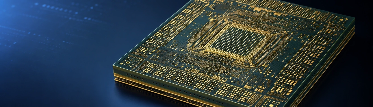
FCBGA Substrates
High-density ABF substrate solutions developed for flip-chip BGA packages requiring fine circuit routing and multilayer interconnection.
CPU and GPU Substrates
Customized build-up substrate structures for processors requiring high interconnection density, reliable signal routing and complex layer configurations.
ASIC and SoC Substrates
Application-specific ABF substrates for ASICs, SoCs and other highly integrated semiconductor packages.
Custom ABF Substrates
Customized ABF substrate solutions developed around package dimensions, layer structure, circuit density and electrical requirements.
ABF Substrates for High-Density Electronic Applications
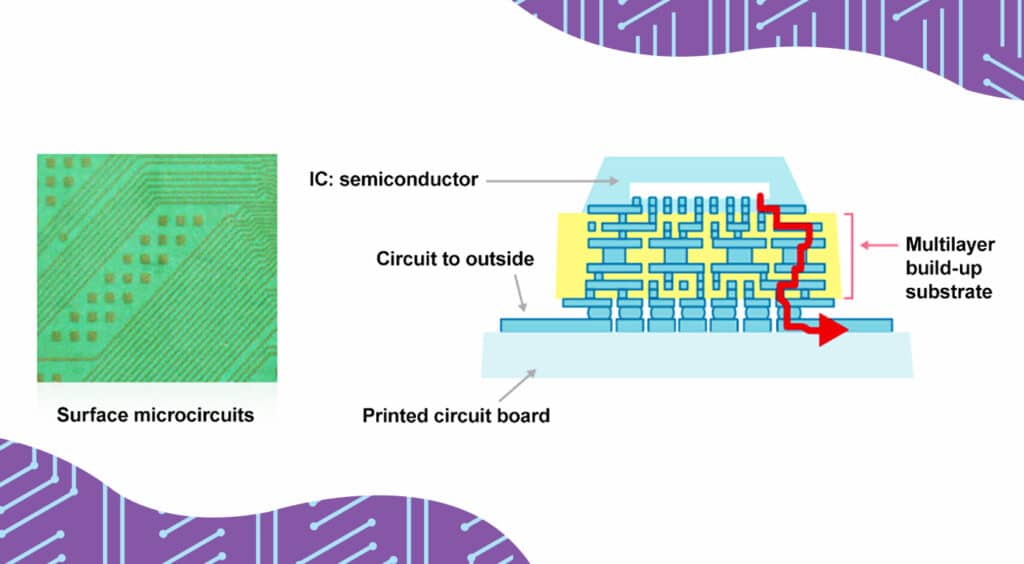
Advanced semiconductor packages require increasingly dense interconnections between fine-pitch chip terminals and system-level printed circuit boards.
ALCANTA provides ABF substrate manufacturing solutions based on package architecture, routing density, build-up structure, electrical requirements and production conditions.
✓ Fine-line circuit capability
✓ Laser microvia structures
✓ Customized build-up layers
✓ Engineering and production support
ABF Substrate Solutions
High-Density Circuit Routing
Fine-line ABF substrates support dense circuit layouts and compact interconnection structures for advanced semiconductor packages.
Typical Applications:
- CPU and GPU Packages
- AI Accelerators
- High-I/O IC Packages
ABF Substrate Manufacturing Capability
| Item | Capability |
|---|---|
| Material | Ajinomoto Build-up Film Systems |
| Line / Space | Down to 9 μm / 9 μm |
| Minimum Laser Via Diameter | Down to 55 μm |
| Layer Count | 2–26 Layers |
| Build-Up Structure | Customized |
| Substrate Thickness | 0.10–3.20 mm |
| Maximum Panel Size | Up to 600 × 600 mm |
| Surface Finish | ENIG, ENEPIG, OSP |
| Quality Control | Electrical and Reliability Testing |
These values represent published BT/ABF manufacturing capabilities for applicable designs.
Actual capability depends on the selected ABF grade, copper thickness, dielectric thickness, package dimensions, layer configuration, via structure and overall design complexity.
Final specifications are confirmed through project-specific engineering review.
From Design Review to Production
Engineering Review
We evaluate the package structure, ABF material requirements, line and space, laser vias, stack-up and manufacturing feasibility before production.
Prototype Validation
Prototype development, dimensional inspection and electrical verification are provided for customized ABF substrate designs.
Volume Production
Validated projects move into repeat or volume production with defined process controls, inspection requirements and production support.
Frequently Asked Questions About ABF Substrates
What is ABF substrate?
An ABF Substrate is a semiconductor package substrate that uses Ajinomoto Build-up Film as an insulating build-up material.
The ABF layers support laser via formation, copper metallization and fine circuit routing between semiconductor chips and printed circuit boards.
What does ABF stand for?
ABF stands for Ajinomoto Build-up Film.
It is an insulating build-up material developed for high-density semiconductor package substrates.
What applications use ABF Substrates?
ABF Substrates are commonly used for CPUs, GPUs, AI accelerators, ASICs, SoCs, network processors and other high-I/O semiconductor packages.
Why is there a shortage of ABF substrate?
ABF enables fine circuit formation, laser microvia processing and multilayer build-up structures.
These capabilities make it suitable for advanced packages requiring dense routing and a high number of chip interconnections.
Can ALCANTA provide customized ABF Substrates?
Yes. ALCANTA evaluates customized ABF Substrates based on package dimensions, layer count, build-up structure, circuit density, via configuration and electrical requirements.
What line and space capability does ALCANTA support?
ALCANTA supports line and space structures down to 9 μm / 9 μm for applicable ABF substrate designs.
Final capability depends on the material grade, copper thickness, layer structure, substrate dimensions and design complexity.
What is the minimum laser via diameter?
Laser via diameters down to 55 μm can be evaluated for suitable designs.
The achievable diameter depends on the ABF dielectric thickness, via structure, aspect ratio and copper-plating requirements.
What files are required for an ABF Substrate quotation?
Customers are recommended to provide:
Gerber or ODB++ files
Package dimensions
Layer count and stack-up
ABF material requirement
Minimum line and space
Laser via diameter
Copper thickness
Surface finish
Prototype and production quantities


