
Custom QFN/QFP Lead Frame in Semiconductor Packaging
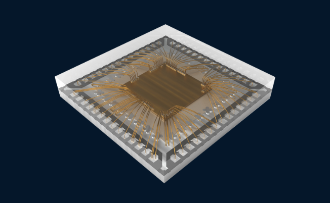
Lead frames are essential components in semiconductor packaging, providing both mechanical support and electrical connections between the silicon chip and the external circuit board. As electronics evolve towards smaller, more powerful devices, the need for advanced lead frame solutions has grown. Custom QFN/QFP Lead Frame designs play a crucial role in this, offering optimized thermal performance, electrical conductivity, and design flexibility. QFN (Quad Flat No-Lead) lead frames are ideal for applications requiring enhanced heat dissipation and reduced signal interference, while QFP (Quad Flat Package) lead frames provide secure soldered connections with extended leads for reliable assembly. The ability to customize these lead frames allows manufacturers to meet specific application needs, improving device performance and longevity. As semiconductor packaging technology advances, custom lead frame solutions will continue to be vital for developing next-generation electronic products.
Understanding Custom QFN/QFP Lead Frame
What is a Custom QFN/QFP Lead Frame?
A lead frame is a crucial component in semiconductor packaging, acting as both the mechanical support and electrical connection for integrated circuits (ICs). It serves as a bridge between the silicon die and the external circuit board, ensuring efficient signal transmission and heat dissipation. Lead frames are widely used in various IC packages, including QFN (Quad Flat No-Lead) and QFP (Quad Flat Package), which are essential for modern electronic devices. The demand for Custom QFN/QFP Lead Frame solutions is increasing as manufacturers seek optimized designs to meet specific application requirements.
Materials Used in Custom QFN/QFP Lead Frame
The material selection for lead frames directly affects their performance, durability, and conductivity. Common materials used in Custom QFN/QFP Lead Frame production include:
- Copper (Cu): Offers excellent electrical conductivity and thermal dissipation, making it the most widely used material.
- Copper Alloys: Enhanced with elements like iron, nickel, or phosphorus to improve mechanical strength and corrosion resistance.
- PPF Lead Frames (Pre-Plated Frames): These feature a protective plating (such as NiPdAu) applied before manufacturing, reducing oxidation and improving solderability.
Manufacturing Processes for Custom QFN/QFP Lead Frame
The production of Custom QFN/QFP Lead Frame involves several advanced techniques to achieve precision and reliability:
- Stamping: A high-speed process where thin metal sheets are punched into the desired lead frame shape. This method is cost-effective for large-scale production.
- Etching: A chemical process that dissolves unwanted metal to create intricate patterns. This technique is ideal for producing fine-pitch lead frames with high precision.
- Plating: The lead frame is coated with materials such as silver (Ag), nickel-palladium-gold (NiPdAu), or tin (Sn) to enhance corrosion resistance, solderability, and electrical performance.
By utilizing these advanced manufacturing techniques, Custom QFN/QFP Lead Frame solutions provide superior performance, ensuring high reliability for semiconductor packaging applications.
Differences Between Custom QFN/QFP Lead Frame
Definition and Characteristics of QFN (Quad Flat No-Lead)
QFN (Quad Flat No-Lead) is a surface-mount integrated circuit (IC) package known for its compact size and excellent thermal and electrical performance. It features a lead frame-based structure where the leads are exposed at the bottom rather than extending outward. This leadless design allows for efficient heat dissipation and minimizes electrical resistance, making QFN packages ideal for high-speed and high-frequency applications.
Custom QFN/QFP Lead Frame designs for QFN packages are widely used in applications that require space-saving solutions and high reliability. The exposed metal pads on the bottom facilitate direct soldering onto the PCB, reducing signal loss and enhancing mechanical stability. Additionally, the absence of extended leads minimizes inductance, which is crucial for high-performance electronics.
Definition and Characteristics of QFP (Quad Flat Package)
QFP (Quad Flat Package) is a traditional leaded IC package where the leads extend outward from all four sides of the package. These thin and flat leads allow for easy soldering and reworkability, making QFP a preferred choice in applications that require robust electrical connections and mechanical stability.
A Custom QFN/QFP Lead Frame for QFP packages typically incorporates high-precision lead structures to ensure consistent solder joint quality. QFP packages are commonly used in microcontrollers, processors, and other semiconductor devices where leaded connections provide better flexibility in assembly and inspection.
Key Differences: Leaded vs. Leadless, Thermal Performance, Assembly Methods
-
Leaded vs. Leadless Design:
- QFN is a leadless package, meaning it does not have extended leads. Instead, it has exposed metal contacts on the bottom, making it more compact.
- QFP, in contrast, features outward-extending leads, which provide greater mechanical flexibility but require more space.
-
Thermal Performance:
- QFN offers superior thermal dissipation due to its exposed bottom pad, allowing direct heat transfer to the PCB. This makes it highly suitable for high-power applications.
- QFP, while still offering decent heat dissipation, relies on the leads for thermal transfer, making it less efficient in comparison to QFN.
-
Assembly Methods:
- QFN requires reflow soldering with precise alignment to ensure all pads make proper contact. Once soldered, it is difficult to inspect and repair.
- QFP is easier to handle and rework due to its visible leads, making it a preferred choice in applications that require frequent adjustments or modifications.
Both QFN and QFP packages have distinct advantages depending on the application. Custom QFN/QFP Lead Frame solutions allow manufacturers to tailor lead frame designs to optimize performance, ensuring the best balance of size, thermal efficiency, and reliability for electronic devices.
Customization of Custom QFN/QFP Lead Frame
Why Custom Lead Frames?
Custom lead frames are essential in modern semiconductor packaging to meet the specific requirements of different applications. A Custom QFN/QFP Lead Frame allows manufacturers to optimize performance, overcome size constraints, and enhance heat dissipation, ensuring reliable and efficient operation of electronic devices.
- Performance Optimization: Tailored lead frames improve electrical conductivity, signal integrity, and mechanical stability, which is critical for high-speed and high-frequency applications.
- Size Constraints: Many electronic devices require compact packaging solutions. A Custom QFN/QFP Lead Frame can be designed with optimized dimensions, allowing for higher circuit density without compromising performance.
- Heat Dissipation: Efficient thermal management is crucial for semiconductor reliability. Custom designs can integrate heat-sinking features such as thermal vias or exposed pads to improve heat dissipation and prevent overheating.
Design Considerations for Custom QFN/QFP Lead Frame
Creating a Custom QFN/QFP Lead Frame involves several design factors to ensure optimal functionality:
- Lead Count & Pitch: The number of leads and the spacing (pitch) between them directly affect connectivity and assembly precision. Fine-pitch designs enable high-density circuits but require advanced manufacturing techniques.
- Material Selection: Copper and copper alloys are commonly used due to their excellent electrical and thermal properties. The choice of material impacts performance, durability, and cost.
- Surface Finish: The surface finish plays a crucial role in solderability and corrosion resistance. Different coatings can be applied depending on the assembly and environmental requirements.
Plating Options and Their Benefits
Plating is a critical step in lead frame manufacturing, enhancing durability, conductivity, and resistance to oxidation. A Custom QFN/QFP Lead Frame can be plated with various materials, each offering distinct advantages:
- Silver (Ag): Provides excellent electrical conductivity and solderability, making it ideal for high-performance applications.
- Nickel-Palladium-Gold (NiPdAu): Offers enhanced corrosion resistance and solderability without requiring lead-based materials, making it environmentally friendly.
- Pre-Plated Frames (PPF): A cost-effective solution where the lead frame is plated before manufacturing, reducing production steps and improving oxidation resistance.
By carefully considering these factors, manufacturers can develop a Custom QFN/QFP Lead Frame that meets specific application needs, ensuring superior performance, reliability, and efficiency in semiconductor packaging.
Manufacturing Process of Custom QFN/QFP Lead Frame
The manufacturing of a Custom QFN/QFP Lead Frame is a complex and precise process that ensures high-quality semiconductor packaging. Various techniques are used to shape, plate, and inspect lead frames to meet specific application requirements. Advanced manufacturing processes such as stamping, etching, and laser cutting are employed to achieve precision, while plating and surface treatments enhance durability and performance. Strict inspection and quality control measures ensure that every Custom QFN/QFP Lead Frame meets industry standards for reliability and efficiency.
Stamping vs. Etching vs. Laser Cutting
-
Stamping:
- Stamping is a high-speed, cost-effective method for mass-producing lead frames.
- A metal sheet is fed into a stamping press, where a die cuts and forms the desired lead frame shape.
- Best suited for designs with standard lead patterns and moderate complexity.
- Can produce high volumes with excellent mechanical strength but may have slight burr formation at the edges.
-
Etching:
- Chemical etching dissolves unwanted metal, creating intricate lead frame patterns with high precision.
- Ideal for fine-pitch designs in Custom QFN/QFP Lead Frame production.
- No mechanical stress or burr formation, resulting in cleaner edges.
- More suitable for prototypes and small to medium production volumes due to higher costs.
-
Laser Cutting:
- Uses high-powered lasers to cut precise lead frame designs.
- Offers extreme accuracy and flexibility in design customization.
- Best for complex, fine-pitch, or high-precision Custom QFN/QFP Lead Frame applications.
- Slower than stamping but highly effective for small batches and specialized designs.
Plating and Surface Treatment Techniques
To enhance performance, Custom QFN/QFP Lead Frame designs undergo various plating and surface treatments:
- Silver (Ag) Plating: Provides excellent electrical conductivity and solderability, commonly used in high-performance applications.
- Nickel-Palladium-Gold (NiPdAu) Plating: Ensures corrosion resistance, improved solderability, and lead-free compliance.
- Pre-Plated Frames (PPF): A cost-effective alternative where plating is applied before the lead frame is processed, reducing oxidation risks.
- Tin (Sn) Plating: Used for improved solderability and environmental resistance.
Inspection and Quality Control
Every Custom QFN/QFP Lead Frame must pass rigorous quality checks to ensure reliability and consistency:
- Dimensional Inspection: Verifies lead frame dimensions, pitch, and alignment using high-precision measurement tools.
- Plating Quality Analysis: Checks coating uniformity, thickness, and adhesion to prevent soldering issues.
- Electrical Conductivity Testing: Ensures low resistance and proper signal transmission for optimal IC performance.
- Thermal Performance Evaluation: Tests heat dissipation capabilities to maintain semiconductor reliability.
By utilizing advanced manufacturing methods and strict quality control, Custom QFN/QFP Lead Frame production ensures that semiconductor packages meet the highest industry standards, supporting the development of high-performance electronic devices.
Applications and Benefits of Custom QFN/QFP Lead Frame
As semiconductor packaging continues to evolve, Custom QFN/QFP Lead Frame solutions play a crucial role in enhancing the performance, durability, and cost efficiency of various electronic applications. Their adaptability to different industries, including consumer electronics, automotive applications, and industrial power electronics, makes them indispensable in modern manufacturing.
Consumer Electronics
In the fast-growing consumer electronics sector, compact and high-performance components are essential. Custom QFN/QFP Lead Frame solutions allow for:
- Smaller, lightweight designs: Essential for smartphones, tablets, and wearable devices.
- Improved thermal management: Ensuring reliable performance in compact devices.
- Enhanced electrical performance: Minimizing signal loss and interference for high-speed processing.
With increasing demand for miniaturized and energy-efficient electronics, Custom QFN/QFP Lead Frame technology helps manufacturers optimize circuit density without compromising quality.
Automotive Applications
Automotive electronics require robust and heat-resistant components to withstand extreme environments. Custom QFN/QFP Lead Frame solutions provide:
- High-temperature resistance: Essential for engine control units (ECUs), sensors, and power management systems.
- Superior mechanical stability: Ensuring durability under continuous vibrations and mechanical stress.
- Reliable electrical connections: Critical for advanced driver-assistance systems (ADAS) and in-vehicle infotainment systems.
With the rise of electric vehicles (EVs) and autonomous driving technologies, Custom QFN/QFP Lead Frame designs are crucial in improving the reliability and efficiency of automotive electronic systems.
Industrial and Power Electronics
Industrial automation, power management, and renewable energy systems require high-efficiency semiconductor components. Custom QFN/QFP Lead Frame technology benefits industrial applications by:
- Enhancing power efficiency: Supporting high-voltage and high-current applications.
- Improving heat dissipation: Essential for power converters, inverters, and motor controllers.
- Providing high durability: Meeting stringent environmental and operational requirements in industrial settings.
These lead frames ensure that industrial equipment operates reliably under demanding conditions, improving productivity and reducing downtime.
Cost Efficiency and Performance Advantages
The adoption of Custom QFN/QFP Lead Frame solutions offers significant cost and performance benefits:
- Reduced manufacturing costs: By optimizing materials and reducing excess packaging.
- Higher assembly efficiency: QFN’s leadless design and QFP’s standard lead configuration simplify PCB mounting.
- Extended product lifespan: Improved thermal management and corrosion resistance enhance the longevity of electronic devices.
- Custom design flexibility: Tailored lead frames allow manufacturers to meet specific application requirements efficiently.
With their superior electrical, thermal, and mechanical properties, Custom QFN/QFP Lead Frame solutions continue to drive advancements across multiple industries, supporting the development of next-generation electronic devices.
Choosing the Right Custom QFN/QFP Lead Frame Manufacturer
Selecting the right manufacturer for a Custom QFN/QFP Lead Frame is a critical decision that impacts the performance, reliability, and cost-effectiveness of semiconductor packaging. With numerous suppliers in the market, businesses must consider key factors such as precision, material quality, and customization capabilities to ensure they receive the best solutions tailored to their needs.
Key Factors in Choosing a Manufacturer
When evaluating a Custom QFN/QFP Lead Frame manufacturer, the following factors should be taken into account:
- Precision and Manufacturing Capabilities: High-precision processes, such as fine-pitch etching, stamping, and plating, are essential for achieving accurate lead frame designs with minimal defects.
- Reliability and Consistency: A trusted manufacturer should have strict quality control measures, including automated inspection systems and rigorous testing to ensure defect-free production.
- Material Quality and Selection: The choice of materials (e.g., copper, copper alloys, PPF lead frames) directly affects thermal performance, conductivity, and durability. The manufacturer should offer a variety of options to meet specific application requirements.
- Cost Efficiency and Scalability: While cost is an important factor, it should not come at the expense of quality. A good supplier will balance affordability with high-quality manufacturing while offering scalability for both small and large production volumes.
- Industry Certifications and Compliance: Manufacturers should adhere to industry standards such as ISO 9001, IATF 16949 (for automotive applications), and RoHS compliance to ensure product safety and reliability.
Leading Suppliers and Service Providers
Several companies specialize in Custom QFN/QFP Lead Frame manufacturing, offering advanced processing techniques and customization options. Some of the industry leaders include:
- ASE Group: A global leader in semiconductor packaging and lead frame production, offering high-precision solutions for various industries.
- Amkor Technology: Specializes in QFN and QFP packaging with high-reliability lead frame solutions.
- Heraeus Electronics: Provides high-performance lead frames with advanced plating technologies.
- Caplinq: Offers a wide range of lead frames, including etched and stamped designs with different plating options.
- QPL Limited: A well-known supplier focusing on high-quality lead frame production with precision etching and stamping techniques.
Each of these manufacturers provides different levels of customization, material choices, and surface treatments, allowing customers to select the best partner based on their specific needs.
How to Work with a Manufacturer for Custom Designs
Developing a Custom QFN/QFP Lead Frame requires close collaboration with the manufacturer. To ensure a smooth process, businesses should follow these steps:
- Define Requirements: Clearly outline the specifications, including lead count, pitch, material preferences, plating options, and thermal performance needs.
- Consult with the Manufacturer: Engage with the supplier’s engineering team to discuss feasibility, design modifications, and cost implications.
- Prototype Development: Request prototypes to test performance, manufacturability, and compliance with PCB assembly requirements.
- Validation and Testing: Work with the manufacturer to conduct electrical, thermal, and mechanical testing to ensure reliability before mass production.
- Mass Production and Quality Assurance: Establish quality control protocols, batch testing, and inspection processes to maintain consistency throughout production.
By selecting a reputable manufacturer and engaging in a structured collaboration process, businesses can ensure that their Custom QFN/QFP Lead Frame meets the highest standards of performance, efficiency, and cost-effectiveness.
FQAs Abut Custom QFN/QFP Lead Frame
What is the difference between QFP and QFN?
- QFP (Quad Flat Package): QFP is a type of IC package with leads that extend outward from all four sides of the package. These leads are used to make electrical connections to the PCB. QFP packages are typically used in applications where the device needs to be accessible for inspection or repair, and they offer robust mechanical connections.
- QFN (Quad Flat No-Lead): QFN is a leadless package where the leads are underneath the package and connect directly to the PCB. QFN packages offer better thermal performance because the bottom pad can be used for heat dissipation, making them ideal for high-performance and high-frequency applications. They are also more compact compared to QFP packages.
How do you make a lead frame?
Lead frames are typically made through a combination of stamping, etching, and laser cutting. The process starts with a metal sheet, usually copper or a copper alloy, which is cut or etched to form the desired pattern for the leads and other components of the frame. Once the lead frame is shaped, it is plated with materials like silver, gold, or nickel to enhance conductivity and solderability. The lead frame is then tested for quality before being used in semiconductor packaging.
What is the difference between QFN and leaded packages?
- QFN (Leadless Package): In a QFN package, there are no external leads. Instead, the electrical connections are made through pads on the bottom of the package that directly connect to the PCB. This design allows for better thermal performance and a more compact package.
- Leaded Packages: Leaded packages, like QFP or DIP (Dual In-line Package), have leads that extend from the sides of the package and connect to the PCB. These packages are easier to handle and inspect but tend to be bulkier and less efficient in terms of heat dissipation compared to leadless designs like QFN.
What are the different types of lead frames?
There are several types of lead frames used in semiconductor packaging:
- Stamped Lead Frames: These are created by pressing metal sheets into specific shapes using a stamping process.
- Etched Lead Frames: These are made by using a chemical etching process to remove material from a metal sheet to form the lead frame.
- Pre-Plated Lead Frames (PPF): These lead frames come pre-plated with a thin metal coating (such as gold or silver) for better conductivity and corrosion resistance.
- Laser-Cut Lead Frames: These are manufactured using laser cutting technology for more intricate designs with fine-pitch leads.
- Ball Grid Array (BGA) Lead Frames: Used in BGA packaging, these lead frames have an array of solder balls instead of leads for connecting to the PCB.

