
Key Advantages of Thin Quad Flat Pack Lead Frame in Electronics
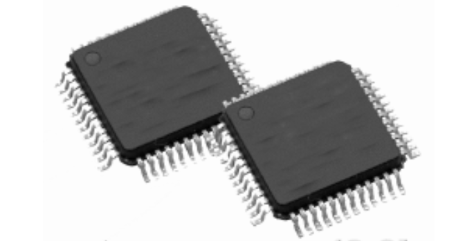
IC packaging is the process of enclosing semiconductor chips in a protective case to ensure electrical connections and mechanical stability. It plays a crucial role in determining the performance, reliability, and integration of integrated circuits (ICs) in electronic devices. One widely used packaging type is the Thin Quad Flat Pack Lead Frame (TQFP), a surface-mount technology that features a square-shaped package with leads extending from all four sides.
This packaging design is specifically created to accommodate high-pin-count ICs while maintaining a thin profile, making it ideal for compact electronic devices. Its lightweight structure, excellent heat dissipation, and ease of PCB assembly contribute to its popularity. The semiconductor industry favors this packaging due to its cost-effectiveness, space efficiency, and reliable electrical performance, making it a preferred choice for consumer electronics, automotive systems, industrial controls, and telecommunications applications.
Basic Structure of Thin Quad Flat Pack Lead Frame
The Thin Quad Flat Pack Lead Frame (TQFP) package is a surface-mount integrated circuit (IC) packaging type designed for high-pin-count applications while maintaining a compact and lightweight structure. It consists of several key components that contribute to its performance and reliability.
Key Components of the Thin Quad Flat Pack Lead Frame Package
- Lead Frame – The core structural element, made of a conductive metal (typically copper or an alloy), which provides mechanical support and electrical connections between the semiconductor die and the printed circuit board (PCB).
- Encapsulation Material – A protective molded plastic that encloses the semiconductor die, safeguarding it from physical damage, moisture, and contaminants.
- Leads – Thin metal extensions protruding from all four sides of the package, enabling electrical connections between the IC and the PCB through surface-mount soldering.
Standard Dimensions and Thickness of Thin Quad Flat Pack Lead Frame
The Thin Quad Flat Pack Lead Frame is designed to be thinner than conventional QFP packages, typically featuring a package thickness between 1.0 mm to 1.4 mm, compared to 1.7 mm to 2.0 mm for standard QFPs. Lead counts vary, generally ranging from 32 to 256 pins, with lead pitches (spacing between leads) commonly available in 0.4 mm, 0.5 mm, 0.65 mm, and 0.8 mm configurations.
Major Differences Between Thin Quad Flat Pack Lead Frame and Conventional QFP
- Thickness – The Thin Quad Flat Pack Lead Frame has a reduced profile compared to conventional QFPs, making it suitable for slim electronic devices.
- Thermal Performance – Due to its thinner profile, it often exhibits improved heat dissipation properties, beneficial for high-performance applications.
- Soldering and Assembly – TQFP’s finer lead pitch enables higher-density PCB designs, allowing more components to be placed within limited board space.
By integrating these structural advantages, this packaging solution offers an optimal balance between compact size, cost-effectiveness, and reliable electrical performance, making it a preferred choice in modern semiconductor packaging.
Features of Thin Quad Flat Pack Lead Frame
The TQFP is a widely used IC packaging type known for its compact size, high pin density, and excellent performance. Designed to meet the demands of modern electronic applications, this package offers significant advantages in terms of space efficiency, functionality, and reliability.
Thin Profile Design Suitable for Compact Electronic Devices
One of the key features of the Thin Quad Flat Pack Lead Frame is its ultra-thin profile, making it ideal for space-constrained electronic devices. Compared to conventional Quad Flat Package (QFP) designs, TQFP has a reduced package thickness, typically ranging from 1.0 mm to 1.4 mm. This thinner profile allows manufacturers to integrate high-performance ICs into sleek and lightweight products such as smartphones, tablets, laptops, and wearables, where reducing form factor is essential.
High Pin Count Capability for Complex ICs
The Thin Quad Flat Pack Lead Frame supports a wide range of pin counts, typically between 32 and 256 pins, with fine-pitch lead spacing options such as 0.4 mm, 0.5 mm, 0.65 mm, and 0.8 mm. This high pin count capability makes TQFP an excellent choice for microcontrollers, digital signal processors (DSPs), and system-on-chip (SoC) solutions that require multiple input/output (I/O) connections. The well-organized lead arrangement on all four sides enhances signal routing efficiency and facilitates high-density PCB layouts, optimizing circuit performance.
Excellent Thermal and Electrical Performance
The packaging is designed to offer superior thermal dissipation and electrical performance. Its lead frame structure, typically made from copper or copper alloys, provides efficient heat conduction, preventing overheating in high-power applications. Additionally, its well-defined lead configuration minimizes parasitic capacitance and inductance, ensuring stable signal transmission and reducing electrical interference. These characteristics make the package particularly suitable for high-speed computing, automotive electronics, and industrial control systems that require reliable thermal and electrical stability.
By combining a thin profile, high pin density, and excellent performance characteristics, the Thin Quad Flat Pack Lead Frame remains a preferred IC packaging solution for a broad range of advanced semiconductor applications.
Manufacturing Process of Thin Quad Flat Pack Lead Frame
The TQFP is manufactured through a series of precise and highly controlled processes to ensure reliability, electrical performance, and durability. Each step in the production of this package plays a crucial role in determining the final quality of the integrated circuit (IC) package.
Lead Frame Fabrication
The manufacturing process begins with the fabrication of the Thin Quad Flat Pack Lead Frame, which serves as the structural foundation of the package. The lead frame is typically made from a highly conductive metal, such as copper or copper alloys, to ensure efficient electrical and thermal performance. The metal sheet undergoes stamping or etching to form the required lead patterns, which define the number of leads and their arrangement. After this, the lead frame is plated with materials such as silver, palladium, or gold, enhancing conductivity and preventing oxidation.
Die Attach and Wire Bonding
Once the lead frame is prepared, the semiconductor die (chip) is securely attached to the die pad using epoxy adhesive or solder paste. This process ensures strong mechanical stability and good thermal conductivity. After die attachment, wire bonding is performed to establish electrical connections between the chip and the leads of the Thin Quad Flat Pack Lead Frame. Thin gold or copper wires, typically 15–35 microns in diameter, are used to bond the die’s contact pads to the lead frame using high-precision ultrasonic or thermosonic bonding technology.
Encapsulation and Package Molding
To protect the delicate die and wire bonds, the package undergoes an encapsulation process. The lead frame assembly is placed into a molding system, where it is encapsulated with an epoxy-based compound that provides mechanical protection, moisture resistance, and thermal insulation. Once the molding process is complete, the package is cured in a high-temperature environment to solidify the encapsulant. Afterward, deflashing and trimming are performed to remove excess molding compound and separate the individual units from the lead frame strip.
Plating, Marking, and Final Testing
After molding, the Thin Quad Flat Pack Lead Frame goes through lead plating, where the leads are coated with a thin layer of tin or other solderable materials to improve soldering performance. Following this, laser marking is used to imprint product details, including the IC model, batch number, and manufacturer’s logo. The final stage involves electrical and functional testing, where each TQFP unit is examined for short circuits, open connections, and performance consistency. Advanced automated optical inspection (AOI) and X-ray inspection are also conducted to detect any hidden defects.
Upon passing all quality control checks, the Thin Quad Flat Pack Lead Frame ICs are packaged and prepared for distribution, ready to be integrated into various high-performance electronic applications.
Comparison with Other IC Packages: Thin Quad Flat Pack Lead Frame vs. Alternatives
The TQFP is a widely used surface-mount IC package, but it is often compared with other packaging types, such as standard QFP, LQFP, and QFN. Understanding these differences helps in selecting the right package for specific applications.
QFP vs. TQFP: Differences in Thickness and Dimensions
The primary distinction between Quad Flat Package (QFP) and Thin Quad Flat Pack Lead Frame is the thickness. Standard QFP packages have a thickness ranging from 1.7 mm to 2.0 mm, whereas TQFP is designed to be much thinner, typically 1.0 mm to 1.4 mm. This reduction in thickness makes TQFP more suitable for compact and lightweight electronic devices, such as smartphones, tablets, and wearables.
While both QFP and TQFP share a square lead arrangement with gull-wing leads extending from all four sides, TQFP generally provides better thermal performance due to its improved heat dissipation features. Manufacturers prefer this packaging type when designing products that require high pin counts while maintaining a low-profile form factor.
TQFP vs. LQFP: Design and Application Distinctions
Both Thin Quad Flat Pack Lead Frame and Low Profile Quad Flat Package (LQFP) are designed to be thinner than traditional QFPs, but LQFP is even thinner than TQFP. LQFP typically has a thickness of 1.0 mm or less, whereas TQFP is slightly thicker at 1.0 mm to 1.4 mm.
LQFP is often used in applications that demand extreme miniaturization, such as portable medical devices, ultra-thin laptops, and high-density embedded systems. On the other hand, this type of packaging strikes a balance between size, pin density, and heat dissipation, making it a more versatile option for consumer electronics, industrial control, and automotive applications.
TQFP vs. QFN: Lead Design and Soldering Differences
The Thin Quad Flat Pack Lead Frame and Quad Flat No-Lead Package (QFN) differ significantly in their lead design and soldering methods. While TQFP has gull-wing leads extending outward, QFN has no protruding leads; instead, its terminals are located on the bottom of the package.
This key difference impacts PCB soldering techniques. TQFP’s gull-wing leads make it easier to inspect and rework using traditional soldering methods, whereas QFN requires X-ray inspection due to its hidden solder joints. Additionally, QFN generally offers better electrical and thermal performance because of its direct thermal pad connection to the PCB, making it suitable for RF modules, power management ICs, and high-speed applications.
The package offers a balanced approach between ease of assembly, pin count, and compactness, making it a preferred choice for a wide range of semiconductor applications compared to QFP, LQFP, and QFN alternatives.
Applications of Thin Quad Flat Pack Lead Frame
The Thin Quad Flat Pack Lead Frame (TQFP) is widely used across various industries due to its compact size, high pin count, and excellent electrical and thermal performance. Its ability to accommodate complex integrated circuits (ICs) while maintaining a low-profile design makes it an ideal choice for applications in consumer electronics, industrial control, telecommunications, and automotive electronics.
Consumer Electronics: Smartphones, Tablets
One of the most significant applications of the Thin Quad Flat Pack Lead Frame is in consumer electronics, where space efficiency and lightweight design are critical. TQFP packages are commonly used in smartphones, tablets, laptops, and gaming consoles to house microcontrollers, power management ICs, and interface chips. Their fine-pitch lead arrangement allows for high-density circuit integration, ensuring efficient signal processing and low power consumption—key factors in battery-operated mobile devices.
Industrial Control: Microcontrollers, DSPs
The packaging solution is a preferred choice for industrial control systems, where microcontrollers and digital signal processors (DSPs) are crucial for automation, robotics, and smart manufacturing. Its high pin count capability allows seamless integration of multiple I/O interfaces, analog-to-digital converters (ADCs), and communication protocols within a single package. Additionally, its excellent thermal dissipation properties ensure reliable operation in high-performance computing and embedded control applications.
Telecommunications: Wireless Modules, RF Chips
In telecommunications, the Thin Quad Flat Pack Lead Frame is extensively used in wireless communication modules, RF (radio frequency) chips, and networking devices. Its robust electrical performance minimizes signal loss and interference, making it ideal for Wi-Fi, Bluetooth, 5G modems, and satellite communication systems. The compact and surface-mountable nature of TQFP also allows for high-speed data processing in network routers, base stations, and IoT (Internet of Things) devices.
Automotive Electronics: ECU (Electronic Control Units), Sensors
The automotive industry increasingly relies on the Thin Quad Flat Pack Lead Frame for Electronic Control Units (ECUs), sensor modules, and engine management systems. With the growing demand for ADAS (Advanced Driver Assistance Systems), electric vehicles (EVs), and autonomous driving technologies, TQFP-based microcontrollers and ICs are used for powertrain control, infotainment systems, and vehicle-to-everything (V2X) communication. The package’s high reliability, vibration resistance, and efficient heat dissipation make it suitable for the harsh conditions of automotive environments.
By offering a balance of compactness, high pin density, and thermal efficiency, this packaging solution remains a leading choice across multiple industries, supporting advancements in consumer electronics, industrial automation, telecommunications, and automotive technology.
Selection and Design Considerations for Thin Quad Flat Pack Lead Frame
Choosing the right Thin Quad Flat Pack Lead Frame (TQFP) package is critical to ensuring optimal performance and compatibility with printed circuit board (PCB) designs. Several key factors must be considered, including selecting the appropriate TQFP specification, ensuring PCB layout compatibility, and following best practices for soldering and rework. Proper design and assembly processes enhance reliability and functionality in various electronic applications.
How to Choose the Right TQFP Specification?
Selecting the appropriate package depends on several technical requirements:
- Pin Count: TQFP packages are available with 32 to 256 pins, with varying lead pitch options such as 0.4 mm, 0.5 mm, 0.65 mm, and 0.8 mm. Higher pin counts are suitable for complex applications like microcontrollers (MCUs) and digital signal processors (DSPs), while lower pin counts work well for simpler integrated circuits.
- Package Thickness: The standard thickness of a Thin Quad Flat Pack Lead Frame typically ranges from 1.0 mm to 1.4 mm, making it important to choose a thickness that aligns with product design constraints, especially in compact applications such as smartphones and embedded systems.
- Thermal Dissipation: TQFP packages are designed for efficient heat dissipation, but some variations may include thermal pads or exposed lead frames to enhance heat transfer. Applications requiring high power levels, such as automotive ECUs and industrial control systems, should prioritize TQFP packages with improved thermal management features.
- Electrical Performance: The choice of package should consider signal integrity and EMI (electromagnetic interference) performance. For high-speed circuits, selecting a component with optimized lead configuration and minimal parasitic effects can significantly enhance electrical performance.
PCB Design Compatibility with TQFP Packages
A well-designed PCB layout is crucial for achieving proper functionality when integrating the Thin Quad Flat Pack Lead Frame package. Key PCB design considerations include:
- Pad Layout and Spacing: The PCB footprint must precisely match the TQFP lead pitch and dimensions to ensure reliable soldering and electrical connections. Adequate spacing should be maintained between adjacent traces to minimize crosstalk and signal interference.
- Thermal Via Placement: For TQFP packages with exposed thermal pads, placing thermal vias directly under the package can enhance heat dissipation, reducing the risk of overheating and performance degradation.
- Solder Mask and Stencil Design: Using a correctly sized solder mask opening prevents solder bridging between leads, while a well-designed stencil aperture ensures uniform solder paste application, improving solder joint quality.
- Ground and Power Planes: Implementing dedicated ground and power planes in multilayer PCBs helps in reducing electrical noise, improving signal stability, and enhancing the performance of high-frequency circuits.
Soldering and Rework Guidelines for TQFP
Proper soldering techniques are essential for ensuring robust connections when assembling the Thin Quad Flat Pack Lead Frame package onto a PCB. Additionally, rework procedures must be carefully executed to avoid damaging the component or PCB.
- Reflow Soldering: TQFP components are typically assembled using reflow soldering, where solder paste is applied to the PCB pads before the package is placed and heated in a controlled temperature profile. Maintaining a peak reflow temperature of 230–260°C ensures proper solder joint formation while preventing thermal stress on the component.
- Hand Soldering Guidelines: While reflow soldering is preferred, TQFP packages can also be soldered manually using fine-tipped soldering irons and flux. A controlled soldering temperature of 350–370°C and a steady hand are required to avoid overheating and misalignment.
- Inspection and Rework: Since Thin Quad Flat Pack Lead Frame packages have fine-pitch leads, automated optical inspection (AOI) and X-ray imaging are commonly used to detect soldering defects such as bridging, cold joints, and insufficient solder. For rework, hot air reflow stations and solder wick can be used to remove excess solder or reflow misaligned components.
- Moisture Sensitivity Considerations: TQFP packages are classified under Moisture Sensitivity Levels (MSL) and require proper storage in dry-packaging or nitrogen cabinets before soldering. Baking the components at 125°C for several hours may be necessary if moisture absorption is suspected, preventing popcorning effects during reflow.
By carefully selecting the right specification, designing a compatible PCB layout, and following best soldering practices, manufacturers can achieve high reliability and performance in their electronic products.
Future Trends in TQFP Technology: Thin Quad Flat Pack Lead Frame
As semiconductor technology continues to evolve, the Thin Quad Flat Pack Lead Frame (TQFP) packaging format is also undergoing significant advancements to meet the increasing demands for higher density, improved performance, and environmental sustainability. Emerging trends in TQFP technology focus on enhancing package density, integrating with advanced packaging solutions, and adopting eco-friendly materials to align with global industry standards.
Advancements in High-Density Packaging
The rapid growth of high-performance computing, AI-driven systems, and IoT devices has driven the need for high-density semiconductor packaging. To meet these requirements, the Thin Quad Flat Pack Lead Frame is being optimized for finer lead pitches, reduced package dimensions, and increased pin counts.
- Finer Pitch Technology: Modern TQFP packages are now being developed with lead pitches as small as 0.3 mm, enabling higher pin densities while maintaining compact form factors. This allows more complex ICs to be integrated into space-constrained electronic designs, such as ultra-thin laptops, wearables, and miniaturized medical devices.
- Enhanced Thermal and Electrical Performance: Future TQFP designs incorporate advanced thermal dissipation techniques, such as integrated heat spreaders and exposed die pads, to improve heat management in high-power applications like automotive control systems and industrial automation. Additionally, low-inductance lead designs help reduce signal interference, making TQFP more suitable for high-frequency and high-speed data processing applications.
- Higher Pin Count Variations: With semiconductor devices requiring more I/O connections, newer versions of this packaging technology are being developed with pin counts exceeding 300, enabling greater functionality while maintaining cost-effective manufacturing processes.
Integration with Advanced Packaging Technologies
As the semiconductor industry shifts towards heterogeneous integration and system-in-package (SiP) solutions, the Thin Quad Flat Pack Lead Frame is being combined with other advanced packaging technologies to improve overall performance and efficiency.
- Hybrid TQFP-BGA Solutions: Ball Grid Array (BGA) technology offers superior electrical performance and thermal dissipation, and new developments are exploring hybrid TQFP-BGA packages that integrate surface-mount leads with ball-grid contacts. This approach enhances signal integrity while maintaining the manufacturability advantages of traditional quad flat pack packaging.
- WLCSP and TQFP Co-Packaging: Wafer-Level Chip Scale Packaging (WLCSP) is another breakthrough that allows for direct die-to-PCB integration. While WLCSP offers a highly compact form factor, it lacks the robust mechanical stability of TQFP. Future trends involve co-packaging WLCSP dies within a TQFP structure, offering both space-saving benefits and enhanced reliability, particularly in automotive and telecommunications applications.
- Embedded Substrate Technology: Innovations in substrate embedding techniques allow TQFP packages to be directly integrated with multi-layer PCB structures, reducing the overall package height while improving thermal efficiency and signal integrity. This is particularly beneficial for AI accelerators, FPGA designs, and high-density microcontroller applications.
Eco-Friendly and Lead-Free TQFP Development
With increasing global regulations on hazardous materials, the Thin Quad Flat Pack Lead Frame is evolving toward more eco-friendly and lead-free manufacturing processes.
- RoHS and REACH Compliance: Modern TQFP packages are now fully compliant with Restriction of Hazardous Substances (RoHS) and Registration, Evaluation, Authorization, and Restriction of Chemicals (REACH) standards, eliminating the use of lead (Pb), cadmium (Cd), and other toxic materials. Lead-free soldering techniques, such as tin-silver-copper (SAC) alloys, are now widely adopted in TQFP assembly.
- Recyclable Encapsulation Materials: Newer TQFP packages use halogen-free molding compounds and bio-based epoxy resins, reducing the environmental impact of semiconductor manufacturing. These materials also enhance moisture resistance and thermal stability, ensuring greater reliability in harsh operating conditions.
- Energy-Efficient Manufacturing: Semiconductor manufacturers are optimizing the fabrication and assembly processes of these packages to reduce energy consumption and carbon footprint. Advanced low-temperature soldering techniques and water-based cleaning processes are now being implemented to make production more sustainable.
The future of the Thin Quad Flat Pack Lead Frame is being shaped by high-density packaging advancements, integration with next-generation semiconductor technologies, and eco-friendly innovations. As electronic devices continue to demand greater functionality in smaller, more power-efficient packages, TQFP remains a versatile and evolving packaging solution that balances performance, reliability, and sustainability.

