Elevating Electronics: The Impact of HDI PCBs
In the rapidly evolving landscape of electronics, High Density Interconnect Printed Circuit Boards (HDI PCBs) have emerged as pivotal components driving innovation. HDI PCBs represent a technological leap forward, offering increased functionality and efficiency in electronic devices. Their significance lies in their ability to accommodate densely packed components, facilitating smaller form factors and enhanced performance in devices ranging from smartphones to medical equipment. As the demand for compact, high-performance electronics continues to soar, HDI PCBs play a crucial role in meeting these requirements. By enabling intricate circuit designs and robust interconnections, HDI PCBs empower engineers to push the boundaries of what’s possible in electronics manufacturing. In this blog, we delve deeper into the intricacies of HDI PCBs, exploring their applications, advantages, and distinguishing features.
What is HDI PCB?
Applications of HDI PCB
HDI PCBs have revolutionized the electronics industry by offering unparalleled design flexibility, compact form factors, and enhanced performance. Their versatility makes them indispensable across a wide range of electronic products. Let’s delve into some of the key applications of HDI PCBs:
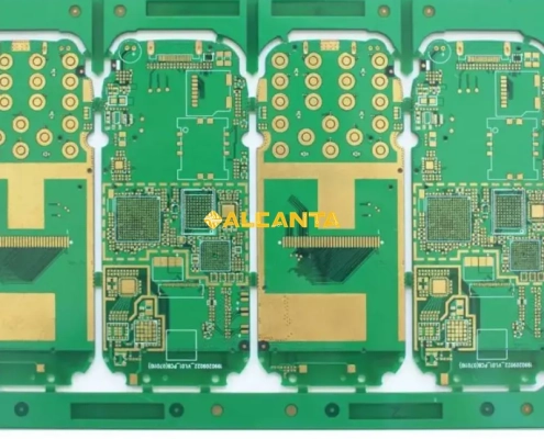
- Smartphones and Tablets: HDI PCBs are extensively used in smartphones and tablets to accommodate the intricate circuitry required for advanced features such as high-resolution displays, multi-touch screens, and high-speed data connectivity. Their compact size and high-density interconnects enable manufacturers to create sleek and lightweight devices without compromising on functionality.
- Medical Devices: In the medical industry, where space is often limited and reliability is paramount, HDI PCBs play a crucial role. They are employed in various medical devices such as patient monitoring systems, diagnostic equipment, implantable devices, and medical imaging devices. HDI PCBs ensure precise signal transmission, compact designs, and reliable performance critical for medical applications.
- Automotive Electronics: With the increasing integration of electronics in modern vehicles, HDI PCBs are in high demand for automotive applications. They are used in advanced driver assistance systems (ADAS), infotainment systems, navigation systems, engine control units (ECUs), and other critical components. HDI PCBs withstand harsh operating conditions, including temperature variations and vibrations, while delivering robust performance.
- Consumer Electronics: HDI PCBs are prevalent in a wide range of consumer electronics beyond smartphones and tablets. They are used in laptops, digital cameras, gaming consoles, wearable devices, and smart home appliances. HDI PCBs enable manufacturers to pack more features into smaller and lighter devices, enhancing user experience and portability.
- Aerospace and Defense: In aerospace and defense applications, where reliability, durability, and performance are non-negotiable, HDI PCBs excel. They are utilized in avionics systems, satellite communications, radar systems, military-grade electronics, and unmanned aerial vehicles (UAVs). HDI PCBs meet stringent quality and reliability standards while offering high-speed data processing capabilities.
- Industrial Equipment: Industrial equipment often requires rugged and compact electronics capable of withstanding harsh environments. HDI PCBs find applications in industrial automation systems, robotics, control panels, and power supplies, where they ensure reliable operation and optimal performance in demanding conditions.
The widespread adoption of HDI PCBs across diverse industries underscores their versatility, reliability, and performance advantages. From consumer electronics to critical applications in medical, automotive, aerospace, and defense sectors, HDI PCBs continue to drive innovation and shape the future of electronic devices.
Difference between HDI PCB and Multilayer PCB
Difference between HDI PCB and IMS PCB
In understanding the difference between HDI PCB (High Density Interconnect Printed Circuit Board) and IMS PCB (Insulated Metal Substrate Printed Circuit Board), it’s essential to grasp their respective characteristics and typical applications.
1. Introduction to IMS PCB:
- IMS PCB, or Insulated Metal Substrate PCB, utilizes a metal substrate (typically aluminum) as the base material with a layer of insulation (usually a thermally conductive dielectric material) sandwiched between the metal substrate and the copper circuit layer. IMS PCBs are designed primarily for applications requiring efficient heat dissipation, making them suitable for high-power electronic devices.
2. Comparison with HDI PCB:
- Application Scenarios:
- HDI PCB: HDI PCBs are more commonly found in electronic devices where space constraints, high component density, and signal integrity are critical factors. They excel in applications such as smartphones, tablets, medical devices, and aerospace electronics, where miniaturization and high performance are paramount.
- IMS PCB: IMS PCBs, on the other hand, are specifically designed for applications requiring effective thermal management. They are commonly used in LED lighting systems, power converters, motor drives, automotive electronics, and other high-power applications where heat dissipation is a concern.
- Functionality:
- HDI PCB: HDI PCBs focus on achieving high-density interconnections and compact designs, enabling the integration of complex circuitry into smaller form factors. They prioritize signal integrity and miniaturization without compromising performance.
- IMS PCB: IMS PCBs prioritize thermal conductivity and heat dissipation. They are engineered to efficiently transfer heat away from sensitive electronic components to prevent overheating and ensure reliable operation, particularly in high-power applications.
- Manufacturing Complexity:
- HDI PCB: HDI PCBs typically involve complex manufacturing processes such as laser drilling, sequential lamination, and via filling to achieve high-density interconnections. This complexity may result in higher manufacturing costs.
- IMS PCB: While IMS PCBs may also require specialized manufacturing techniques, such as metal substrate fabrication and dielectric layer bonding, their complexity is primarily focused on optimizing thermal performance rather than interconnection density.
- Cost Considerations:
- HDI PCB: Due to their complex manufacturing processes and high-density interconnections, HDI PCBs may incur higher manufacturing costs compared to standard PCBs.
- IMS PCB: IMS PCBs may also involve additional manufacturing steps and material costs associated with the metal substrate and thermal interface materials, potentially impacting overall production costs.
In summary, while both HDI PCBs and IMS PCBs serve critical roles in electronic design, their applications and priorities differ significantly. HDI PCBs focus on high-density interconnections and miniaturization for compact electronic devices, while IMS PCBs prioritize thermal management for high-power applications. Understanding these differences is crucial for selecting the appropriate PCB technology to meet specific design requirements and performance objectives.
Difference between HDI PCB and FR4
When contrasting HDI PCB (High Density Interconnect Printed Circuit Board) with FR4, it’s essential to delve into their distinctive characteristics, considering their substrate material, line density, cost implications, manufacturing complexity, and other factors.
1. Introduction to FR4:
- FR4 is a widely used substrate material for PCBs, renowned for its cost-effectiveness, versatility, and electrical insulation properties. It consists of a woven fiberglass cloth impregnated with epoxy resin, providing mechanical strength and electrical insulation to the PCB.
2. Comparison with HDI PCB:
- Substrate Material:
- HDI PCB: HDI PCBs can utilize various substrate materials, including specialized high-performance materials tailored for specific applications. These substrates often feature advanced properties such as enhanced thermal conductivity, low dielectric loss, and improved signal integrity.
- FR4: FR4 is the most common substrate material used in conventional PCBs due to its affordability and availability. While FR4 offers adequate electrical insulation and mechanical strength, it may not possess the advanced properties required for high-performance applications.
- Line Density:
- HDI PCB: HDI PCBs excel in achieving high line densities, allowing for more intricate and densely packed circuitry within a smaller footprint. This enables the creation of compact electronic devices with enhanced functionality.
- FR4: Traditional FR4 PCBs typically have lower line densities compared to HDI PCBs, limiting their ability to accommodate complex designs and high component densities. This may result in larger PCB sizes and less efficient use of space.
- Cost Implications:
- HDI PCB: Due to their advanced manufacturing processes, specialized materials, and higher line densities, HDI PCBs tend to be more expensive to produce compared to standard FR4 PCBs. However, the cost may be justified by the enhanced performance and functionality offered by HDI PCBs.
- FR4: FR4 PCBs are known for their cost-effectiveness, making them a preferred choice for applications where strict budget constraints are a concern. The lower cost of FR4 PCBs is attributed to the widespread availability of FR4 substrate materials and the simplicity of their manufacturing processes.
- Manufacturing Complexity:
- HDI PCB: HDI PCBs involve complex manufacturing processes such as laser drilling, sequential lamination, and via filling to achieve high-density interconnections. These processes require specialized equipment and expertise, contributing to higher manufacturing complexity.
- FR4: Manufacturing FR4 PCBs is relatively straightforward and involves standard processes such as etching, drilling, and solder masking. The simplicity of FR4 PCB manufacturing contributes to shorter lead times and lower production costs compared to HDI PCBs.
In summary, while both HDI PCBs and FR4 PCBs serve essential roles in electronic design, they differ significantly in substrate material, line density, cost implications, and manufacturing complexity. HDI PCBs offer advantages in terms of higher line densities and advanced performance characteristics, albeit at a higher cost and manufacturing complexity compared to FR4 PCBs. Understanding these differences is crucial for selecting the appropriate PCB technology to meet specific design requirements and performance objectives.
FAQs About HDI PCB
What is HDI in PCBs?
HDI, or High Density Interconnect, in PCBs refers to a technology that enables the creation of densely packed circuitry with multiple layers, microvias, and advanced interconnect techniques. HDI PCBs offer higher line densities and smaller form factors compared to traditional PCBs.
What is the difference between HDI and PTH PCB?
HDI PCBs utilize advanced interconnect technologies such as microvias, buried vias, and sequential lamination to achieve high-density interconnections. PTH (Plated Through-Hole) PCBs, on the other hand, rely on through-hole vias that penetrate the entire board thickness. HDI PCBs offer higher line densities and better signal integrity compared to PTH PCBs.
What is high density PCB board?
A high density PCB board refers to a printed circuit board with a high number of components and interconnections per unit area. These boards are characterized by their compact size, intricate circuitry, and advanced manufacturing techniques, such as HDI technology, to achieve high-density interconnects.
What is the difference between HDI and FR4?
HDI (High Density Interconnect) refers to a technology used in PCBs to achieve high-density interconnections and compact designs. FR4, on the other hand, is a type of substrate material commonly used in PCB manufacturing, known for its affordability and versatility. While HDI denotes a specific PCB technology, FR4 refers to a substrate material choice.


