
Comparing Semiconductor Package Substrate and PCBs
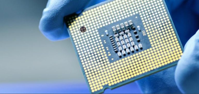
Semiconductor packaging is a critical process in the electronics industry, serving as the bridge between the semiconductor chip and the external environment. It involves encasing the semiconductor die in a protective package that facilitates electrical connections and provides mechanical support. The importance of semiconductor packaging cannot be overstated, as it affects the performance, reliability, and longevity of electronic devices.
A semiconductor package substrate is a fundamental component within this packaging system. It provides a physical platform for mounting the semiconductor die and establishes the necessary electrical connections between the die and the printed circuit board (PCB). The substrate also helps dissipate heat generated during operation and protects the delicate semiconductor from environmental factors. Understanding the role and materials of semiconductor package substrates is essential for optimizing device performance and ensuring long-term reliability.
Overview of Semiconductor Package Substrates
What is a Semiconductor Package Substrate?
A semiconductor package substrate is a vital component used in the packaging of semiconductor devices, such as integrated circuits (ICs). It serves as the foundation on which the semiconductor die is mounted and provides the necessary connections between the die and the external circuitry.
Definition and Function
In technical terms, a semiconductor package substrate is a laminated structure typically made from materials such as epoxy resins, ceramic, or high-frequency laminates. It consists of multiple layers, including conductive traces, dielectric layers, and sometimes embedded components. The primary function of the substrate is to support the semiconductor die mechanically and electrically. It facilitates the routing of electrical signals between the die and the package’s external pins or balls, enabling communication with the rest of the electronic system. Additionally, the substrate helps in thermal management by dispersing heat generated by the semiconductor device during operation.
Role in Electronic Devices
The semiconductor package substrate plays a crucial role in the performance and reliability of electronic devices. By providing a stable platform for the semiconductor die, it ensures secure mounting and reduces the risk of damage from mechanical stresses. The substrate’s electrical traces are designed to maintain signal integrity and minimize interference, which is essential for high-speed and high-frequency applications. Furthermore, effective thermal management through the substrate is vital for preventing overheating, which can adversely affect the performance and lifespan of the semiconductor device. In essence, the package substrate is integral to the overall functionality and durability of electronic systems.
Materials Used in Semiconductor Package Substrates
Types of Package Substrate Materials
Semiconductor package substrates are made from various materials, each offering unique properties that suit different applications. The choice of material affects the performance, reliability, and cost of the semiconductor package.
Common Materials
- FR-4 (Flame Retardant 4)
- Characteristics: FR-4 is a widely used material in PCB and semiconductor packaging, composed of woven glass fabric and epoxy resin. It is known for its electrical insulation properties and moderate thermal conductivity.
- Advantages: FR-4 is cost-effective, offers good mechanical strength, and is easy to process. It provides adequate performance for many general-purpose applications.
- Disadvantages: It has limited thermal management capabilities and lower performance at high frequencies. FR-4 substrates may not be suitable for high-speed or high-power applications.
- BT (Bismaleimide-Triazine)
- Characteristics: BT resin is a high-performance material used in advanced semiconductor packaging. It is a thermosetting polymer with good thermal stability and low moisture absorption.
- Advantages: BT substrates offer superior thermal and mechanical properties, low electrical loss, and are well-suited for high-speed and high-frequency applications. They also exhibit excellent dimensional stability.
- Disadvantages: BT materials are more expensive than FR-4 and require more complex processing, which can increase manufacturing costs.
- High-Frequency Materials
- Characteristics: High-frequency materials, such as PTFE (Polytetrafluoroethylene) and ceramics, are designed to handle high-speed signal transmission with minimal loss and interference.
- Advantages: These materials have low dielectric constants and loss tangents, which reduce signal degradation and improve performance in high-frequency and high-speed applications. They also offer excellent thermal stability.
- Disadvantages: High-frequency materials are generally more costly and may require specialized manufacturing techniques. They can also be more brittle and challenging to handle compared to FR-4 and BT.
Characteristics, Advantages, and Disadvantages
- FR-4: Offers a balance of cost and performance for general applications but falls short in high-frequency or high-power scenarios due to its thermal and electrical limitations.
- BT: Provides excellent performance in high-speed and high-frequency applications with superior thermal stability, though it comes at a higher cost and complexity.
- High-Frequency Materials: Essential for advanced electronic systems requiring optimal signal integrity and thermal performance. However, they are typically more expensive and may require advanced processing techniques.
Choosing the appropriate substrate material depends on the specific requirements of the semiconductor package, including cost constraints, performance needs, and application environments.
Comparison: Package Substrate vs. PCB
Package Substrate vs. PCB
Package substrates and printed circuit boards (PCBs) are both essential components in electronic systems, but they serve distinct purposes and exhibit different characteristics. Understanding their key differences helps in selecting the right material for specific applications.
Key Differences
- Structure
- Package Substrate: A package substrate typically has a multi-layered construction with an emphasis on precise, high-density interconnections between the semiconductor die and the package’s external contacts. It includes conductive traces embedded within dielectric layers and often features additional elements like heat spreaders or embedded components. The focus is on supporting the semiconductor die, managing heat, and ensuring reliable electrical connections.
- PCB: A PCB, on the other hand, is usually a single or multi-layered board designed to interconnect various electronic components within a system. It features conductive tracks, pads, and vias on a flat board, which facilitates the routing of electrical signals between components. PCBs are generally less complex than package substrates and focus more on providing mechanical support and signal routing for a broad range of components.
- Use
- Package Substrate: Used primarily in the packaging of semiconductor devices, such as integrated circuits (ICs). It is critical for mounting the semiconductor die, establishing electrical connections between the die and external pins or balls, and managing heat dissipation. Package substrates are integral to ensuring the performance and reliability of the semiconductor device within the final electronic product.
- PCB: Used to create the main platform for mounting and connecting a variety of electronic components, such as resistors, capacitors, and ICs, in electronic devices. PCBs are used in everything from simple consumer electronics to complex industrial systems, providing the necessary interconnections and mechanical support for the entire electronic circuit.
- Performance
- Package Substrate: Designed to handle high-density, high-frequency, and high-power applications. It must manage the heat generated by the semiconductor die, ensure minimal signal loss, and maintain electrical integrity under various operating conditions. The performance of a package substrate directly impacts the functionality and longevity of the semiconductor device.
- PCB: Performance is more focused on the overall routing of signals and power distribution within a device. While high-frequency and high-speed applications require advanced PCB materials and designs, PCBs generally prioritize cost, manufacturability, and versatility in connecting various components.
Applications of Each
- Package Substrate: Commonly used in semiconductor packaging technologies such as Ball Grid Array (BGA), Flip-Chip Ball Grid Array (FCBGA), and Chip-on-Board (COB). These substrates are crucial for applications requiring precise electrical and thermal management, such as processors, memory modules, and other high-performance ICs.
- PCB: Found in a wide range of electronic products, from simple gadgets like remote controls to complex devices like computer motherboards and automotive control systems. PCBs are integral to almost all electronic devices, providing the necessary connections and support for various components to function together effectively.
While both package substrates and PCBs are essential for electronic systems, package substrates are specialized for semiconductor packaging with a focus on high-density interconnections and thermal management, whereas PCBs are more generalized platforms for connecting and supporting electronic components.
Uses of Semiconductor Package Substrates
Applications of Semiconductor Package Substrates
Semiconductor package substrates are crucial in various applications where precise electrical and thermal management is required. They play a key role in ensuring the reliability and performance of electronic devices by providing a stable platform for semiconductor die and facilitating connections to external circuitry.
Typical Applications
- IC Packaging
- Description: Integrated Circuit (IC) packaging is the most common application for semiconductor package substrates. This involves encasing the semiconductor die in a protective package that includes the substrate. The substrate provides the necessary electrical connections between the die’s internal circuitry and the external pins or balls.
- Types: Various IC packages use different substrates, such as Dual In-line Package (DIP), Surface Mount Device (SMD), and Chip-on-Board (COB). Each type has specific requirements for substrate performance based on factors like pin count, signal speed, and power handling.
- Ball Grid Array (BGA)
- Description: BGA is a popular packaging method where the package substrate has an array of solder balls on the underside, which are used to connect the package to the PCB. The package substrate in BGA provides high-density interconnections and improved thermal performance.
- Advantages: BGA substrates support higher pin counts and improved heat dissipation compared to traditional package types. They are used in a wide range of applications, from consumer electronics to automotive systems.
- Flip-Chip Ball Grid Array (FCBGA)
- Description: FCBGA is a variation of BGA where the semiconductor die is mounted face-down on the package substrate. The die’s bumps or balls make direct contact with the substrate’s pads, enabling high-density interconnections.
- Advantages: FCBGA substrates offer better electrical performance and thermal management due to the close proximity of the die to the substrate. This package type is commonly used in high-performance processors and memory devices.
- Chip-on-Board (COB)
- Description: COB involves directly bonding the semiconductor die onto the PCB or a dedicated substrate. The die is connected to the PCB using wire bonds or flip-chip bumps.
- Advantages: COB substrates are used for applications where compact size and cost are critical. They are commonly found in LED lighting, consumer electronics, and some automotive applications.
Impact on Electronic Device Performance
- Electrical Performance: The choice of package substrate material and design significantly impacts the electrical performance of the semiconductor device. High-quality substrates ensure minimal signal loss, reduced electromagnetic interference, and stable electrical connections, which are crucial for high-speed and high-frequency applications. Inadequate substrate performance can lead to signal degradation, increased power consumption, and operational failures.
- Thermal Management: Effective thermal management is another critical factor influenced by the package substrate. Substrates with good thermal conductivity help dissipate heat generated by the semiconductor die, preventing overheating and potential damage. Poor thermal management can result in reduced device performance, shorter lifespan, and reliability issues.
- Mechanical Stability: The mechanical stability provided by the package substrate ensures that the semiconductor die is securely mounted and protected from physical stresses during operation and handling. This stability is vital for maintaining the integrity of electrical connections and preventing mechanical failures.
Semiconductor package substrates are integral to the performance and reliability of electronic devices, impacting electrical performance, thermal management, and mechanical stability. Their applications range from basic IC packaging to advanced BGA and FCBGA technologies, each tailored to meet specific requirements and performance standards.
Semiconductor Package Substrate Manufacturers
Key Manufacturers
The semiconductor package substrate industry is characterized by several key players that provide a range of advanced substrates to meet the diverse needs of electronic applications. These leading companies are known for their expertise in materials, manufacturing processes, and technological innovations.
Introduction to Leading Companies
- ASE Group (Advanced Semiconductor Engineering)
- Overview: ASE Group is one of the largest semiconductor packaging and testing service providers globally. Established in 1984, ASE has extensive experience in semiconductor packaging solutions and is renowned for its high-quality substrates and advanced packaging technologies.
- Products and Services: ASE offers a wide array of semiconductor package substrates, including BGA, FCBGA, and CSP (Chip Scale Package) substrates. The company provides comprehensive services, including design support, prototyping, and high-volume manufacturing. ASE is known for its advanced thermal management solutions and high-density interconnect technologies.
- Amkor Technology
- Overview: Founded in 1968, Amkor Technology is a leading provider of semiconductor packaging and test services. Amkor is recognized for its extensive portfolio of packaging solutions and its global manufacturing footprint.
- Products and Services: Amkor specializes in various package substrates, including BGAs, FCBGAs, and other advanced packages. The company offers services such as package design, assembly, and testing. Amkor’s focus is on delivering high-performance packaging solutions with advanced features such as fine-pitch interconnects and improved thermal dissipation.
- JCET Group (Jiangsu Changjiang Electronics Technology Co., Ltd.)
- Overview: JCET Group is one of the largest semiconductor packaging and testing companies in China. Established in 1972, JCET is known for its innovation and extensive product offerings in the semiconductor packaging industry.
- Products and Services: JCET provides a broad range of package substrates, including advanced BGA, FCBGA, and SIP (System-in-Package) solutions. The company offers end-to-end services, from substrate design and development to mass production and testing. JCET is noted for its capabilities in high-density interconnects and high-performance packaging.
- Taiwan Semiconductor Manufacturing Company (TSMC)
- Overview: TSMC, founded in 1987, is a leading semiconductor foundry known for its advanced wafer fabrication services. In addition to its core wafer manufacturing, TSMC is involved in the development and supply of semiconductor package substrates.
- Products and Services: TSMC offers a variety of package substrates, including advanced BGA, FCBGA, and CoWoS (Chip-on-Wafer-on-Substrate) solutions. The company provides integrated services that include design, packaging, and testing, with a focus on cutting-edge technologies and high-performance solutions.
- Shenzhen Fastprint Circuit Tech Co., Ltd.
- Overview: Shenzhen Fastprint is a prominent PCB and semiconductor packaging substrate manufacturer based in China. Established in 1999, the company specializes in high-quality substrates and PCB solutions.
- Products and Services: Fastprint offers a range of semiconductor package substrates, including FR-4, BT, and high-frequency materials. The company provides services such as custom substrate design, prototyping, and mass production, focusing on delivering reliable and cost-effective solutions.
Products and Services Offered
- Package Substrates: Leading manufacturers provide various substrate types, including BGA, FCBGA, CSP, and SIP packages. These substrates are designed to support different levels of complexity and performance requirements in semiconductor devices.
- Design and Prototyping: Many manufacturers offer design and prototyping services to help customers develop custom substrate solutions tailored to specific needs. This includes assistance with material selection, layout design, and thermal and electrical optimization.
- High-Volume Manufacturing: Key players in the industry have extensive manufacturing capabilities to produce substrates at high volumes while maintaining quality and performance standards. This includes advanced fabrication techniques, quality control processes, and scalable production lines.
- Testing and Support: Manufacturers often provide comprehensive testing services to ensure the reliability and functionality of semiconductor packages. This includes electrical testing, thermal analysis, and mechanical inspections. Additionally, technical support and consultation services are available to assist with substrate design and integration.
Leading semiconductor package substrate manufacturers play a critical role in advancing packaging technologies and providing high-performance solutions for a wide range of electronic applications. Their products and services are essential for ensuring the functionality, reliability, and efficiency of semiconductor devices in modern electronics.
Types of Package Substrates
Types of IC Package Substrates
IC package substrates come in various types, each designed to meet specific performance and application requirements. Understanding these types helps in selecting the right package substrate for a given semiconductor device.
Common Types
- Flip-Chip Ball Grid Array (FC-BGA)
- Description: FC-BGA is a type of package where the semiconductor die is mounted face-down on the substrate. The die’s bumps or balls make direct contact with the substrate’s pads, facilitating high-density interconnections.
- Suitability: FC-BGA is well-suited for high-performance applications that require excellent electrical performance and thermal management, such as processors, memory chips, and high-speed communication devices.
- Pros:
- High Performance: Provides better electrical performance and signal integrity due to the shorter interconnects between the die and the substrate.
- Thermal Management: Effective in heat dissipation, which helps in maintaining device reliability and performance.
- Compact Design: Enables high-density packaging, which is beneficial for space-constrained applications.
- Cons:
- Complex Manufacturing: More complex and costly to manufacture compared to traditional package types.
- Brittleness: The die can be more susceptible to mechanical stress during handling and assembly.
- Chip Scale Package (CSP)
- Description: CSP is a type of packaging where the package size is close to that of the semiconductor die itself. It features an array of solder balls on the bottom of the package, similar to BGA.
- Suitability: CSP is ideal for applications requiring compact and lightweight packages, such as mobile devices, wearable electronics, and consumer gadgets.
- Pros:
- Small Size: Reduces the overall footprint, making it suitable for compact electronic devices.
- Improved Electrical Performance: Offers good electrical performance with shorter interconnects.
- Cost-Effective: Generally more cost-effective than more complex packaging types.
- Cons:
- Limited Heat Dissipation: May have less effective thermal management compared to larger package types.
- Less Robust: Can be more susceptible to thermal and mechanical stresses due to its compact size.
- Land Grid Array (LGA)
- Description: LGA is a package where the semiconductor die is mounted on a substrate with a grid of flat pads or lands that make contact with the PCB through solder joints.
- Suitability: LGA is commonly used for high-pin-count applications such as microprocessors and high-performance ICs where a robust connection and high-density interconnects are required.
- Pros:
- High Pin Count: Supports a large number of connections, which is advantageous for complex ICs.
- Mechanical Stability: Provides good mechanical stability and can handle higher levels of stress.
- Thermal Performance: Can be designed with advanced thermal management features.
- Cons:
- Size: Larger footprint compared to some other package types, which may not be suitable for space-constrained applications.
- Complex Assembly: Requires precise alignment during assembly, which can increase manufacturing complexity.
- Dual In-line Package (DIP)
- Description: DIP is a traditional package with two parallel rows of pins extending from either side of the package. It is one of the oldest and most widely used package types.
- Suitability: DIP is typically used in through-hole applications where the package is inserted into holes on a PCB and soldered on the opposite side. Common in older electronic devices and prototyping.
- Pros:
- Ease of Assembly: Simple to assemble and widely used in prototype and low-volume applications.
- Good Mechanical Strength: Provides robust mechanical support.
- Cost-Effective: Generally less expensive to produce and assemble.
- Cons:
- Limited Density: Not suitable for high-density or high-performance applications due to its large size and limited pin count.
- Poor High-Frequency Performance: Not ideal for high-speed or high-frequency applications due to longer signal paths.
- System-in-Package (SiP)
- Description: SiP integrates multiple ICs or components into a single package, providing a compact and comprehensive solution for complex electronic systems.
- Suitability: Ideal for applications requiring multiple functionalities in a small form factor, such as smartphones, IoT devices, and advanced consumer electronics.
- Pros:
- Compact Integration: Allows for the integration of multiple components, reducing overall system size.
- Enhanced Performance: Provides improved performance through reduced interconnect lengths and integrated design.
- Customization: Offers flexibility in combining different types of components.
- Cons:
- Complex Design: Requires careful design and integration of multiple components, which can increase complexity.
- Higher Cost: Typically more expensive due to the complexity and integration of various elements.
In summary, each type of package substrate offers distinct advantages and limitations. The choice of substrate type depends on factors such as performance requirements, space constraints, thermal management needs, and cost considerations.
Market Trends and Future Developments
Market Trends and Future Directions
The semiconductor package substrate industry is evolving rapidly, driven by the increasing demand for advanced electronic devices and the need for improved performance and miniaturization. Several key market trends and future directions are shaping the industry’s landscape.
Innovations and Technological Advancements
- High-Density Interconnects (HDI)
- Overview: HDI technology allows for the creation of substrates with higher pin counts and smaller feature sizes, enabling more complex and compact designs.
- Advancements: Innovations in HDI include finer line widths and spaces, advanced via technologies, and improved material properties. These advancements facilitate the development of smaller and more powerful electronic devices.
- Impact: HDI substrates are crucial for high-performance applications such as smartphones, tablets, and wearables, where space is limited and performance requirements are high.
- Advanced Packaging Technologies
- Overview: The industry is seeing a shift towards advanced packaging technologies, including 3D packaging, System-in-Package (SiP), and heterogeneous integration.
- Advancements: Technologies like 3D-IC stacking, where multiple ICs are stacked vertically, and SiP, which integrates multiple functionalities into a single package, are becoming more prevalent. Innovations also include improved interconnect technologies and enhanced thermal management solutions.
- Impact: These technologies address the need for increased functionality and reduced size, offering improved performance and efficiency in compact designs.
- Flexible and Printed Electronics
- Overview: Flexible substrates, such as those used in flexible and printed electronics, are gaining traction for applications requiring bendable and lightweight components.
- Advancements: Innovations in materials and printing technologies are enabling the production of flexible substrates with enhanced electrical properties and durability. This includes advances in organic and hybrid materials that offer flexibility and performance.
- Impact: Flexible substrates are used in applications such as wearable electronics, flexible displays, and smart packaging, providing new possibilities for device design and functionality.
- Thermal Management Solutions
- Overview: Effective thermal management is critical for maintaining the performance and reliability of high-power and high-frequency devices.
- Advancements: Recent developments include advanced thermal interface materials (TIMs), improved heat spreader designs, and the use of new materials with better thermal conductivity. These innovations help manage heat dissipation more effectively.
- Impact: Enhanced thermal management solutions ensure the reliability and longevity of high-performance electronic devices, especially in demanding applications such as data centers and automotive systems.
Potential Future Developments
- Integration of Emerging Technologies
- Overview: Future developments may include the integration of emerging technologies such as artificial intelligence (AI) and machine learning (ML) into packaging design and manufacturing processes.
- Potential: AI and ML can optimize design processes, predict failure modes, and enhance quality control. These technologies may lead to more efficient and cost-effective substrate manufacturing.
- Expansion of 5G and Beyond
- Overview: The rollout of 5G technology and future generations of wireless communication will drive demand for advanced substrates capable of supporting high-frequency and high-speed applications.
- Potential: Developments in materials and design techniques will be necessary to meet the performance requirements of 5G and beyond, including improved signal integrity, reduced electromagnetic interference, and enhanced thermal management.
- Sustainability and Green Technologies
- Overview: There is a growing emphasis on sustainability and environmental impact in the electronics industry. Future developments will focus on reducing the environmental footprint of packaging materials and processes.
- Potential: Innovations may include the use of recyclable and biodegradable materials, energy-efficient manufacturing processes, and the reduction of hazardous substances in substrates. These efforts will contribute to a more sustainable electronics industry.
- Advancements in Substrate Materials
- Overview: Ongoing research and development are likely to lead to the creation of new substrate materials with enhanced properties, such as higher thermal conductivity, better electrical performance, and greater flexibility.
- Potential: Advances in material science could lead to the development of substrates that support more demanding applications, such as ultra-high-speed computing, advanced automotive systems, and next-generation consumer electronics.
The semiconductor package substrate industry is poised for significant advancements driven by technological innovations, evolving market needs, and a focus on sustainability. Future developments will likely focus on enhancing performance, integrating emerging technologies, and addressing environmental concerns, shaping the future of electronic device packaging.
FAQs About semiconductor package substrate
A semiconductor packaging substrate is a critical component that provides a platform for mounting and connecting semiconductor devices, such as integrated circuits (ICs), to the printed circuit board (PCB). It ensures electrical connectivity, mechanical stability, and thermal management between the semiconductor die and the external connections or pins.
Substrates for IC packages include various materials and designs, such as:Ball Grid Array (BGA): Features an array of solder balls for high-density interconnections.
Flip-Chip Ball Grid Array (FCBGA): The die is mounted face-down with bumps connecting to the substrate.
Chip Scale Package (CSP): The package size is close to the die size, often used for compact applications.
Land Grid Array (LGA): Uses a grid of flat pads for connections.
System-in-Package (SiP): Integrates multiple components within a single package.
Substrate: The substrate is the underlying material that provides the electrical and mechanical support for mounting semiconductor components and establishing connections. It includes layers of dielectric and conductive materials designed to support the semiconductor die and facilitate electrical connections.
Package: The package encompasses the entire assembly that includes the substrate, the semiconductor die, and the external connections or pins. It provides protection for the die, connects it to the PCB, and often includes features for thermal management.
Substrate materials for packaging vary based on the requirements of the application. Common materials include:FR-4: A widely used fiberglass-epoxy laminate for standard PCBs.
BT (Bismaleimide-Triazine): Offers higher thermal and electrical performance, often used in high-frequency applications.
High-Frequency Materials: Such as Rogers materials, used for applications requiring low signal loss and high performance.
Ceramics: For high-performance applications needing excellent thermal and electrical properties.

