
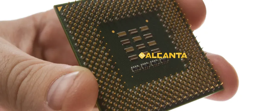
Key Materials in Interposer Substrates and Their Benefits
An Interposer Substrate serves as a vital intermediary in integrated circuits, facilitating connections between different semiconductor components or between a semiconductor and a package substrate. Its role is crucial in enhancing performance, enabling denser integration, and managing thermal and electrical properties effectively. Interposers enable advanced packaging techniques like CoWoS (Chip-on-Wafer-on-Substrate), enabling higher bandwidth and lower power consumption in devices. They bridge the gap between heterogeneous technologies, optimizing signal integrity and reducing latency. In modern electronics, Interposer Substrates are pivotal for achieving compact, high-performance designs in applications ranging from high-speed computing to telecommunications and beyond.
Difference Between Interposer and Package Substrate
Definition and Functions Comparison of Interposer and Package Substrate
An Interposer is an integrated circuit (IC) component that acts as a bridge between different semiconductor devices or between a semiconductor device and a package substrate. It typically contains through-silicon vias (TSVs) or other interconnects to facilitate high-density connections. Interposers are designed to optimize signal routing, manage thermal dissipation, and enhance electrical performance in complex IC designs.
A Package Substrate, on the other hand, serves as a foundation for mounting and interconnecting various components within a semiconductor package. It provides structural support and electrical connections between the semiconductor die and external circuitry. Package substrates are crucial for distributing power, managing heat, and ensuring reliable electrical connections.
Selection Criteria Based on Different Application Scenarios
– Complexity and Integration: Interposers are chosen for applications requiring high-density interconnects and complex signal routing, such as in multi-chip modules and 3D IC stacking. Package substrates are preferred for simpler integration needs where standard packaging solutions suffice.
– Performance Requirements: Interposers excel in applications demanding high-speed data transfer, low latency, and efficient power distribution, benefiting from technologies like TSVs and advanced material properties. Package substrates are suitable for applications with less stringent performance demands, focusing more on cost-effectiveness and reliability.
– Manufacturing Considerations: Interposers involve sophisticated manufacturing processes due to their high-density interconnects and material requirements. Package substrates typically follow standard PCB manufacturing practices but may incorporate advanced materials for enhanced thermal management and reliability.
Understanding these distinctions helps in selecting the most suitable solution based on the specific requirements of the application, balancing performance, cost, and manufacturability considerations effectively.
Types of Interposers
Comparison Between Silicon Interposer and RDL (Redistribution Layer) Interposer
Silicon Interposer: Silicon interposers are fabricated using silicon wafers and often incorporate through-silicon vias (TSVs) to provide vertical connections between stacked dies. They are known for their high-density interconnect capability, enabling complex integration of multiple chips within a compact space. Silicon interposers offer excellent electrical performance, low signal loss, and efficient thermal dissipation due to the inherent properties of silicon.
RDL Interposer (Redistribution Layer): RDL interposers utilize thin-film redistribution layers to reroute connections and redistribute signals between stacked dies or between dies and the package substrate. They are versatile in adapting to various die sizes and configurations, facilitating flexible routing of signals without the need for TSVs. RDL interposers are suitable for applications where cost-effective integration and scalability are priorities, offering reduced manufacturing complexity compared to silicon interposers.
Introduction to CoWoS (Chip-on-Wafer-on-Substrate) Technology and Its Advantages
CoWoS (Chip-on-Wafer-on-Substrate) technology involves stacking multiple silicon chips (known as chiplets) vertically on a silicon interposer or substrate. The interposer serves as a bridge between the chips, enabling high-bandwidth communication with minimal latency. CoWoS technology leverages the capabilities of silicon interposers to achieve superior performance in terms of data transfer rates, power efficiency, and overall system integration.
Advantages of CoWoS Technology:
– High Bandwidth: Enables high-speed data transfer between stacked chips, optimizing performance in applications like high-performance computing and networking.
– Reduced Power Consumption: Efficient signal routing and thermal management contribute to lower power consumption compared to traditional packaging methods.
– Scalability: Facilitates modular design and scalability by allowing integration of diverse chip functionalities (chiplets) on a single substrate, enhancing design flexibility and time-to-market.
Understanding these types of interposers and CoWoS technology aids in selecting the appropriate solution for achieving specific performance goals and integration requirements in advanced semiconductor applications.
Interposer Module
Definition and Applications of Interposer Module
An Interposer Module refers to a complete integrated circuit (IC) package that incorporates an interposer as a central component. It serves as a platform for assembling and interconnecting multiple semiconductor chips or chiplets within a single package. The interposer within the module facilitates high-density interconnects and efficient signal routing between the chips, enhancing overall system performance and functionality.
Applications of Interposer Module:
– High-Performance Computing (HPC): Interposer modules are extensively used in HPC applications to integrate multiple processors, memory modules, and accelerators in a compact and efficient manner. They enable high-bandwidth communication and reduce latency, crucial for data-intensive tasks.
– Networking and Telecommunications: In network infrastructure and telecommunications equipment, interposer modules help integrate diverse functionalities such as processing units, networking chips, and memory modules. They support faster data processing and transmission, improving network efficiency and reliability.
– Consumer Electronics: Interposer modules find applications in consumer electronics, particularly in devices requiring compact designs with enhanced processing capabilities. Examples include high-end smartphones, tablets, and portable gaming consoles where space-saving and performance optimization are critical.
Relationship Between Chiplet Integration and Interposer Module
Chiplet integration refers to the assembly of multiple small semiconductor dies (chiplets) onto a common substrate or interposer within an interposer module. The interposer acts as a bridge, facilitating electrical connections and signal routing between the chiplets and external circuitry. This integration approach allows for modular design, where different chiplets with specialized functions (such as CPUs, GPUs, and memory units) can be combined to create customized IC solutions tailored to specific application requirements.
Advantages of Chiplet Integration with Interposer Module:
– Modular Design: Facilitates flexible configuration and scalability by mixing and matching chiplets to meet diverse application needs.
– Performance Optimization: Enables optimization of power consumption, heat dissipation, and signal integrity by strategically placing chiplets and optimizing interconnect design.
– Cost Efficiency: Reduces overall manufacturing costs by leveraging standardized chiplets and modular assembly processes, enhancing yield and time-to-market for new products.
By leveraging chiplet integration and interposer modules, semiconductor manufacturers can achieve significant advancements in performance, efficiency, and flexibility, catering to the evolving demands of modern electronics and computing systems.
Materials Used in Interposers
Common Types of Materials Used in Interposer Substrates
Interposer substrates utilize various materials tailored to meet specific performance, thermal management, and integration requirements:
– Silicon: Silicon is widely used for its excellent electrical properties, thermal conductivity, and compatibility with semiconductor processes. Silicon interposers often incorporate through-silicon vias (TSVs) for vertical connections between stacked dies.
– Glass: Glass substrates offer high dimensional stability, low thermal expansion coefficients, and good electrical insulation properties. They are suitable for applications requiring high reliability and precise alignment.
– Organic Substrates (e.g., PCB materials): Organic substrates like laminates and build-up films are cost-effective options for interposers. They provide flexibility in design and integration, although they may have limitations in terms of thermal conductivity and electrical performance compared to silicon or glass.
– Ceramics: Ceramics such as alumina (Al2O3) and aluminum nitride (AlN) offer superior thermal conductivity and mechanical stability. They are ideal for applications demanding efficient heat dissipation and reliability in harsh environments.
Characteristics and Suitability Analysis of Various Materials in Interposers
– Electrical Performance: Silicon and ceramics exhibit excellent electrical properties, ensuring minimal signal loss and high-speed signal transmission. Organic materials may have higher losses but are sufficient for many applications.
– Thermal Management: Ceramics and certain types of glass have superior thermal conductivity, enabling efficient heat dissipation in high-power applications. Silicon also offers good thermal management capabilities.
– Manufacturability: Silicon and organic substrates are well-established in semiconductor manufacturing processes, allowing for high-volume production. Ceramics require specialized manufacturing techniques but offer unique benefits in terms of reliability and performance.
– Cost Considerations: Organic substrates are generally more cost-effective than silicon or ceramics, making them suitable for consumer electronics and other cost-sensitive applications. Silicon and ceramics are favored in high-performance computing and telecommunications despite higher manufacturing costs.
Selecting the appropriate material for an interposer substrate depends on balancing these factors with specific application requirements, ensuring optimal performance, reliability, and cost-effectiveness in the final product design.
Manufacturing Processes and Design Guidelines
Overview of Interposer Manufacturing Processes
Interposer manufacturing involves several key processes to ensure the precision, reliability, and functionality of the final product:
– Substrate Preparation: Depending on the chosen material (e.g., silicon, glass, ceramics), substrates are prepared with precise dimensions and surface quality suitable for subsequent processing steps.
– Photolithography: This process involves transferring circuit patterns onto the substrate using photoresist masks and UV light. It defines the layout of interconnects and vias crucial for electrical connections.
– Deposition of Metal Layers: Metal layers, typically composed of materials like copper or aluminum, are deposited onto the substrate through techniques such as physical vapor deposition (PVD) or chemical vapor deposition (CVD). These layers form conductive pathways and interconnects.
– Etching: Etching processes selectively remove unwanted metal or substrate material, defining the shape and structure of interconnects and vias according to the designed patterns.
– Via Formation: Through-silicon vias (TSVs) or microvias are created to establish vertical connections between different layers or chips within the interposer. TSVs in silicon interposers, for example, are crucial for enabling 3D integration and efficient signal routing.
– Assembly and Bonding: Chips or chiplets are bonded onto the interposer substrate using advanced bonding techniques such as flip-chip bonding or wire bonding. This step ensures secure electrical connections and proper alignment between components.
– Testing and Quality Assurance: Comprehensive testing protocols are employed to verify electrical functionality, signal integrity, and thermal performance of the interposer before integration into larger systems.
Key Factors and Guidelines to Consider When Designing Interposers
Designing effective interposers requires careful consideration of several factors to optimize performance, reliability, and manufacturability:
– Signal Integrity: Minimizing signal loss and interference through careful routing and design of interconnects, vias, and signal paths.
– Thermal Management: Efficient heat dissipation through the substrate material and integration of thermal management solutions such as thermal vias or heatsinks.
– Mechanical Stability: Ensuring structural integrity and reliability under mechanical stresses and environmental conditions.
– Electrical Compatibility: Adhering to electrical standards and ensuring compatibility with interfacing components and systems.
– Manufacturability: Designing for ease of manufacturing, including considerations for yield, scalability, and cost-effectiveness.
– Integration Flexibility: Designing interfaces and interconnects that allow for flexible integration of multiple chips or chiplets while maintaining high performance and reliability.
By integrating these considerations into the design process, engineers can develop interposers that meet stringent performance requirements across a wide range of applications, from high-performance computing to consumer electronics and telecommunications.
FAQs about interposer substrate
Package substrate connects semiconductor devices to external circuits.
Interposer facilitates connections between chips or between chips and package substrate.
An interposer module integrates multiple chips using an interposer as a bridge for connections.
Common materials include silicon, glass, ceramics, and organic substrates like PCB materials.
Interposer substrate refers to the base material (like silicon or glass) that forms the foundation for an interposer’s circuitry and connections.

