
How Substrate Like PCB Technology Enhances Performanc
In the dynamic realm of electronics, Printed Circuit Boards (PCBs) are the foundation of nearly every device, from smartphones to industrial equipment. They play a vital role in providing the necessary mechanical support and electrical connections for seamless component functionality. The evolution of PCB technology has significantly enhanced performance, size, and cost efficiency, driving the miniaturization and reliability of modern electronics. This progress has also led to the development of various substrate technologies, expanding the possibilities in electronics design. A substrate in electronics serves as the base material for building electronic components and circuitry, crucially impacting the device’s performance and durability. In PCBs, materials like FR4 (fiberglass-reinforced epoxy laminate) are commonly used for their excellent support and insulation properties. Essentially, PCBs serve as the platform for mounting and interconnecting electronic components, forming the core of any electronic system. This evolution underscores the importance of substrates in advancing electronic technology.
Understanding PCB Technology
What is PCB?
Definition and Basic Function A Printed Circuit Board (PCB) is a board used in electronics to mechanically support and electrically connect electronic components using conductive pathways, or traces, etched from copper sheets laminated onto a non-conductive substrate. The primary function of a PCB is to hold the components of an electronic device in place and provide the necessary electrical connections between them. This allows for the creation of complex electronic circuits in a compact and efficient manner.
Common Materials Used The most common materials used in PCB manufacturing include:
- FR4: This is the most widely used material, consisting of a fiberglass-reinforced epoxy laminate. It offers excellent mechanical strength, electrical insulation, and flame resistance.
- Polyimide: Known for its high heat resistance, flexibility, and durability, polyimide is often used in flexible and high-temperature applications.
- CEM-1 and CEM-3: Composite epoxy materials that are cheaper alternatives to FR4, used in less demanding applications.
Substrate in PCB
Definition and Role of Substrate in PCB In the context of PCBs, the substrate refers to the base material upon which the conductive pathways and electronic components are mounted. The substrate provides the structural support for the board and ensures the electrical insulation between different conductive layers. The choice of substrate material directly impacts the performance, durability, and application of the PCB.
Common Substrate Materials
- FR4: As mentioned, this is the most common substrate material due to its balance of cost, performance, and durability.
- CEM-1: A paper-based laminate with a single layer of woven glass fabric, offering lower cost but reduced performance compared to FR4.
- CEM-3: Similar to CEM-1 but with improved mechanical and thermal properties, making it suitable for slightly more demanding applications.
Difference Between PCB and Substrate
Clarifying the Distinction A PCB is a complete assembly that includes the substrate as its foundational layer, along with etched copper traces, vias, and mounted electronic components. In contrast, the substrate is specifically the base material upon which the entire PCB structure is built. While the PCB encompasses all layers and components, the substrate refers only to the supporting material.
Importance of Substrate in PCB Performance and Reliability The choice of substrate material is critical to the overall performance and reliability of a PCB. The substrate must provide the necessary mechanical support to prevent warping or breaking while ensuring adequate electrical insulation to prevent short circuits. Additionally, the substrate’s thermal properties are essential in managing heat dissipation and maintaining the stability of the electronic components. High-quality substrates like FR4 ensure that the PCB can withstand mechanical stresses, high temperatures, and environmental factors, ultimately contributing to the longevity and dependability of the electronic device.
Types of Substrate Technologies
IC Substrate
Definition and Applications An IC substrate, or Integrated Circuit substrate, is a type of substrate used specifically for mounting integrated circuits. It acts as a bridge between the IC and the printed circuit board, providing the necessary electrical connections and mechanical support. IC substrates are typically used in advanced electronics, including semiconductor packages, microprocessors, and other high-performance devices.
Differences from Traditional PCBs IC substrates differ from traditional PCBs in several key aspects:
- Material Composition: IC substrates often use high-performance materials like BT resin, Ajinomoto Build-up Film (ABF), or liquid crystal polymer (LCP), which offer superior electrical and thermal properties compared to standard PCB materials like FR4.
- Miniaturization: IC substrates are designed to support the miniaturization of electronic components, featuring finer lines and spaces, higher layer counts, and more complex interconnections.
- Manufacturing Processes: The manufacturing of IC substrates involves advanced techniques such as laser drilling and electroplating to achieve the high precision required for semiconductor applications.
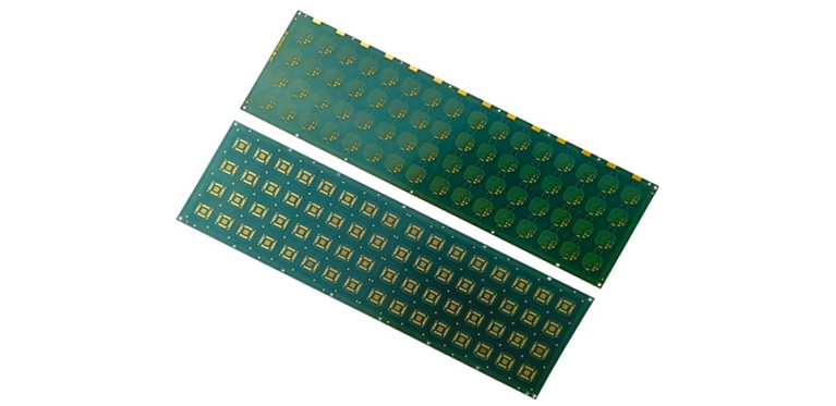
SLP (Substrate-like PCB)
Definition and How It Differs from Standard PCBs SLP, or Substrate-like PCB, is a type of PCB technology that bridges the gap between traditional PCBs and IC substrates. SLPs utilize advanced manufacturing processes similar to those used for IC substrates, resulting in finer lines and spaces, higher density interconnections, and improved electrical performance.
Applications and Benefits of SLP Technology
- Applications: SLP technology is primarily used in high-density applications such as smartphones, tablets, and wearable devices, where space and performance are critical.
- Benefits:
- Higher Density Interconnections: SLPs can achieve much finer lines and spaces, allowing for more interconnections in a smaller area.
- Improved Signal Integrity: The advanced materials and manufacturing processes used in SLPs enhance signal integrity and reduce electrical losses.
- Enhanced Mechanical Strength: SLPs offer better mechanical properties, making them more durable and reliable in compact, high-performance devices.
InPack PCB Technologies
Explanation and Significance InPack PCB technologies refer to integrated packaging technologies that incorporate various functions within a single package. This approach allows for the integration of multiple components, such as ICs, passives, and other elements, into a single, compact package. InPack technologies are significant because they enable higher levels of integration, improved performance, and reduced overall system size.
Differences and Advantages Over Traditional PCB Substrates
- Integration Level: InPack technologies integrate multiple functions and components within a single package, reducing the need for separate PCBs and interconnections.
- Performance: The high level of integration improves electrical performance by reducing signal losses and parasitic effects.
- Size and Weight: InPack solutions can significantly reduce the size and weight of electronic devices by eliminating the need for multiple PCBs and interconnects.
- Manufacturing Efficiency: By integrating components into a single package, InPack technologies streamline the manufacturing process, potentially reducing costs and increasing production efficiency.
IC substrates, SLPs, and InPack PCB technologies represent advanced substrate technologies that address the increasing demand for miniaturization, high performance, and integration in modern electronics. Each of these technologies offers unique advantages and is tailored for specific applications, pushing the boundaries of what is possible in electronics design and manufacturing.
Comparative Analysis
PCB vs. SLP
Key Differences in Structure and Performance
- Structure: Traditional PCBs (Printed Circuit Boards) typically use materials like FR4, with etched copper traces and a standard manufacturing process. They generally feature thicker traces and larger components. SLP (Substrate-like PCB) technology, on the other hand, utilizes advanced materials and manufacturing techniques similar to those used for IC substrates. SLPs have finer lines and spaces, allowing for higher density interconnections and more compact designs.
- Performance: The performance of SLPs is superior in terms of signal integrity, electrical performance, and thermal management. SLPs can handle higher frequencies and provide better impedance control, making them suitable for high-speed applications. Traditional PCBs may struggle with these demands due to their larger trace sizes and less sophisticated materials.
Use Cases Where SLP is Preferred Over Traditional PCBs
- Smartphones and Tablets: The compact size and high performance of SLPs make them ideal for use in mobile devices where space is at a premium and high-speed data transmission is required.
- Wearable Devices: Wearable technology benefits from the small form factor and reliability of SLPs, which can support the complex circuitry needed in a compact space.
- High-Density Applications: Any application requiring high-density interconnections, such as advanced medical devices, automotive electronics, and high-performance computing, can benefit from the use of SLPs.
IC Substrate vs. PCB
Specific Use Cases and Advantages of IC Substrates
- Semiconductor Packaging: IC substrates are critical in semiconductor packaging, providing the necessary interconnections between the chip and the PCB. They offer high-density interconnections and support the miniaturization of semiconductor devices.
- High-Performance Computing: In applications requiring high-speed data processing and transmission, such as servers and data centers, IC substrates provide the necessary performance and reliability.
- Consumer Electronics: IC substrates are widely used in advanced consumer electronics, including smartphones, tablets, and gaming consoles, where performance and compact size are crucial.
How IC Substrates Complement or Replace Traditional PCBs in Certain Applications
- Complementing Traditional PCBs: In many applications, IC substrates are used in conjunction with traditional PCBs to provide high-density interconnections between the chip and the main board. This combination allows for optimal performance and reliability in complex electronic systems.
- Replacing Traditional PCBs: In highly integrated systems, IC substrates can sometimes replace traditional PCBs altogether. For instance, in system-in-package (SiP) and system-on-chip (SoC) applications, IC substrates integrate multiple functions within a single package, reducing the need for separate PCBs and interconnections.
- Advanced Packaging Solutions: IC substrates are integral to advanced packaging solutions like flip-chip and wafer-level packaging, which offer superior electrical performance and thermal management compared to traditional PCB-based packaging.
While traditional PCBs remain widely used in many applications, advanced substrate technologies like SLPs and IC substrates provide significant advantages in terms of performance, size, and integration. These technologies are crucial for meeting the increasing demands of modern electronics, enabling the development of smaller, faster, and more reliable devices.
Future of PCB and Substrate Technologies
Emerging Technologies
Next-Generation Substrate Materials and Technologies
- Advanced Composite Materials: Future PCBs and substrates will increasingly use advanced composite materials like liquid crystal polymer (LCP), ceramic-filled polymers, and flexible organic substrates. These materials offer superior thermal stability, reduced signal loss, and enhanced flexibility, making them ideal for high-frequency and high-density applications.
- Nanotechnology: The incorporation of nanomaterials, such as carbon nanotubes and graphene, holds promise for significantly improving the electrical, thermal, and mechanical properties of PCBs and substrates. These materials can enable the development of ultra-thin, lightweight, and highly conductive circuits.
- High-Density Interconnect (HDI) Technology: HDI technology will continue to evolve, allowing for even finer lines and spaces, more layers, and more complex interconnections. This will be crucial for supporting the miniaturization of electronic devices and the increasing complexity of circuits.
Innovations in PCB Design and Manufacturing
- Additive Manufacturing: Also known as 3D printing, additive manufacturing is poised to revolutionize PCB production. This technology allows for the creation of complex geometries, multi-material assemblies, and rapid prototyping, significantly reducing production times and costs.
- Embedded Components: The trend of embedding passive and active components directly into the PCB substrate will continue to grow. This approach improves performance, reduces board size, and enhances reliability by minimizing solder joints and interconnections.
- Flexible and Stretchable Electronics: Innovations in flexible and stretchable PCB technologies will enable new applications in wearable devices, medical implants, and flexible displays. These technologies use materials that maintain conductivity and functionality while being bent, stretched, or twisted.
Market Trends
Current Trends in Substrate and PCB Technology
- Miniaturization: The demand for smaller, lighter, and more powerful electronic devices drives the trend towards miniaturization. This requires advancements in substrate and PCB technologies to accommodate higher component densities and more intricate designs.
- High-Frequency Applications: As the adoption of 5G, IoT, and other high-frequency technologies grows, there is an increasing need for substrates and PCBs that can handle higher frequencies with minimal signal loss and interference.
- Environmental Sustainability: The electronics industry is focusing more on sustainability, with a push towards eco-friendly materials and manufacturing processes. This includes the development of biodegradable substrates and the reduction of harmful chemicals in PCB production.
Future Outlook and Potential Developments
- Integration of Photonics: The integration of photonics and electronics on a single substrate is a promising area of development. This could lead to faster data transfer rates and improved performance in applications like data centers and telecommunications.
- AI and Machine Learning in PCB Design: The use of artificial intelligence (AI) and machine learning in PCB design and manufacturing will enhance design optimization, fault detection, and production efficiency. AI-driven tools can quickly analyze vast amounts of data to create optimized PCB layouts and predict potential issues.
- Hybrid Electronics: The combination of traditional electronic components with organic and printed electronics will lead to the development of hybrid systems. These systems will leverage the best properties of each type of component to create more versatile and efficient devices.
- Advanced Thermal Management: As electronic devices become more powerful, effective thermal management will be crucial. Innovations in substrate materials and PCB designs will focus on enhancing heat dissipation and maintaining device performance and reliability.
- Quantum Computing: The development of quantum computing will drive the need for entirely new types of substrates and PCBs that can support the unique requirements of quantum circuits, such as maintaining coherence and minimizing noise.
The future of PCB and substrate technologies is marked by rapid advancements and innovative solutions. Emerging materials, new manufacturing techniques, and the integration of cutting-edge technologies will address the increasing demands for miniaturization, performance, and sustainability in the electronics industry. As these trends continue to evolve, they will pave the way for the next generation of electronic devices, transforming industries and everyday life.
FAQs About substrate like pcb technology
No, a PCB (Printed Circuit Board) is not the same as a substrate. A PCB is a complete assembly that includes multiple layers, including the substrate, conductive pathways, vias, and mounted electronic components. The substrate is specifically the base material of the PCB, providing mechanical support and electrical insulation for the conductive pathways and components. While the PCB encompasses all these elements, the substrate is just one component, albeit a crucial one, within the overall structure.
PCB (Printed Circuit Board):
Structure: Typically uses materials like FR4, with copper traces etched on the substrate. PCBs can be single-sided, double-sided, or multi-layered, depending on the complexity of the circuit.
Performance: Standard PCBs are suitable for a wide range of applications but may have limitations in high-frequency or high-density applications due to larger trace sizes and less sophisticated materials.
Applications: Used in a broad spectrum of electronic devices, from consumer electronics to industrial machinery.
SLP (Substrate-like PCB):
Structure: Uses advanced manufacturing techniques similar to IC substrates, with finer lines and spaces, allowing for higher density interconnections.
Performance: SLPs offer better signal integrity, higher electrical performance, and improved thermal management compared to standard PCBs. They are designed to handle higher frequencies and more complex circuitry.
Applications: Ideal for high-density applications such as smartphones, tablets, wearable devices, and other compact, high-performance electronics.
Common substrate materials used in PCBs include:
FR4: The most widely used material, made from fiberglass-reinforced epoxy laminate. It offers a good balance of mechanical strength, electrical insulation, and thermal resistance.
Polyimide: Known for its high heat resistance, flexibility, and durability, making it suitable for flexible and high-temperature applications.
CEM-1 and CEM-3: Composite epoxy materials that are cost-effective alternatives to FR4, used in less demanding applications. CEM-1 is a paper-based laminate with a single layer of woven glass fabric, while CEM-3 is similar but with improved mechanical and thermal properties.
BT Resin: Used in IC substrates, offering superior electrical and thermal properties.
Ceramic: Used in high-frequency and high-power applications due to its excellent thermal conductivity and electrical insulation properties.
The next-generation technologies that are emerging alongside or as alternatives to traditional PCBs include:
High-Density Interconnect (HDI) Technology: Allows for finer lines and spaces, higher layer counts, and more complex interconnections, supporting the miniaturization of electronic devices.
Flexible and Stretchable Electronics: Use materials that maintain conductivity and functionality while being bent, stretched, or twisted, enabling new applications in wearables, medical devices, and flexible displays.
3D Printing/Additive Manufacturing: Revolutionizes PCB production by enabling the creation of complex geometries, multi-material assemblies, and rapid prototyping, significantly reducing production times and costs.
Embedded Components: Embedding passive and active components directly into the PCB substrate improves performance, reduces board size, and enhances reliability by minimizing solder joints and interconnections.
Photonics Integration: Combining photonics and electronics on a single substrate for faster data transfer rates and improved performance, particularly in data centers and telecommunications.
Organic and Printed Electronics: Combining traditional components with organic materials and printed electronics for more versatile and efficient devices.
Advanced Thermal Management Solutions: Developing new substrate materials and PCB designs to enhance heat dissipation and maintain device performance and reliability.
Quantum Computing: Requiring new types of substrates and PCBs to support the unique requirements of quantum circuits, such as maintaining coherence and minimizing noise.
These emerging technologies aim to address the increasing demands for miniaturization, performance, and sustainability in the electronics industry, paving the way for the next generation of electronic devices.

