
SKC Glass Substrate: Enhancing Semiconductor Packaging
In the realm of advanced packaging technology, SKC glass substrate stands as a pivotal element, driving innovation and efficiency in semiconductor manufacturing processes. This blog aims to delve into the multifaceted significance of SKC glass substrate, elucidating its role as a cornerstone of modern packaging solutions. Structured to offer a comprehensive understanding, our discussion will unfold in three key sections. Firstly, we’ll delve into the manufacturer, highlighting SKC’s expertise and leadership in the industry. Following that, we’ll explore the diverse applications where SKC glass substrate shines, from chip packaging to advanced configurations like Chip-on-Wafer-on-Substrate (CoWoS). Finally, we’ll delve into the technical intricacies, uncovering the unique features and advantages that make SKC glass substrate indispensable in high-density integrated circuit packaging. Join us on this journey to uncover the essence of SKC glass substrate and its transformative impact on semiconductor packaging technology.
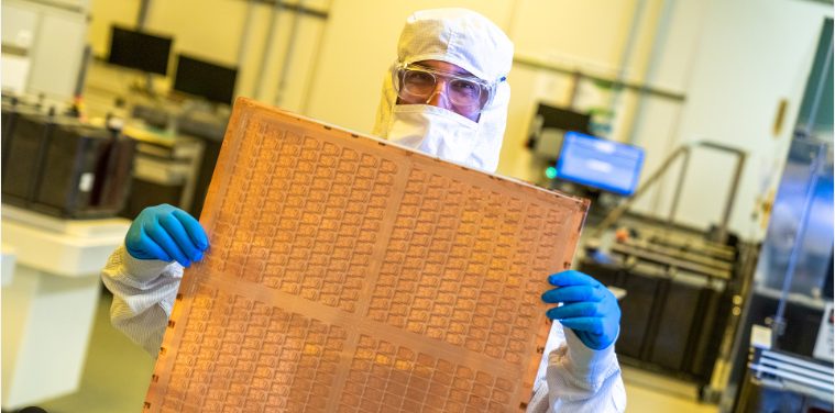
Manufacturer of SKC Glass Substrate
SKC, a pioneering force in the realm of glass substrate manufacturing, stands prominently as one of the foremost leaders globally. Established on a foundation of innovation and excellence, SKC has garnered a reputation for pushing the boundaries of what’s possible in semiconductor packaging technology. With state-of-the-art facilities and a commitment to research and development, SKC has consistently delivered cutting-edge solutions tailored to the evolving needs of the industry.
SKC’s expertise in glass substrate fabrication is unmatched, underpinned by decades of experience and a relentless pursuit of quality and precision. Their advanced manufacturing processes, coupled with stringent quality control measures, ensure that each substrate meets the highest standards of performance and reliability.
Moreover, SKC’s leading position in the glass substrate field is underscored by its proactive approach to collaboration and partnership. By working closely with semiconductor companies, research institutions, and technology leaders, SKC continuously refines its products and processes, staying ahead of the curve in an ever-evolving industry landscape.
In essence, SKC’s commitment to innovation, coupled with its unparalleled expertise and leading-edge technology, solidifies its status as a trailblazer in glass substrate manufacturing, shaping the future of advanced packaging solutions worldwide.
Applications of SKC Glass Substrate
SKC glass substrate serves as a linchpin in the landscape of advanced packaging technology, finding versatile applications across various domains. Its remarkable properties and precision engineering make it indispensable in a multitude of scenarios, ranging from traditional chip packaging to cutting-edge configurations like Chip-on-Wafer-on-Substrate (CoWoS).
In chip packaging, SKC glass substrate plays a pivotal role in providing a reliable and robust foundation for semiconductor devices. Its high thermal conductivity ensures efficient heat dissipation, which is crucial for maintaining optimal performance and extending the lifespan of chips. Additionally, SKC glass substrate’s excellent dimensional stability and electrical insulation properties contribute to the overall reliability and functionality of packaged chips.
In advanced packaging, SKC glass substrate emerges as a key enabler of miniaturization and integration. Its superior dielectric properties facilitate the implementation of intricate circuitry in compact form factors, allowing for denser and more powerful electronic devices. Furthermore, SKC glass substrate’s compatibility with advanced manufacturing processes such as flip-chip bonding and through-silicon vias (TSVs) further enhances its utility in advanced packaging applications.
Moreover, in the realm of Chip-on-Wafer-on-Substrate (CoWoS) packaging, SKC glass substrate shines as a cornerstone technology. By providing a stable platform for stacking multiple dies vertically, SKC glass substrate enables the creation of high-performance, multi-chip modules with unprecedented levels of integration. This innovative packaging approach not only enhances performance and functionality but also offers significant advantages in terms of size, weight, and power consumption.
In summary, SKC glass substrate’s versatility, reliability, and advanced properties make it an indispensable component in modern semiconductor packaging. Whether in traditional chip packaging, advanced configurations, or pioneering CoWoS technology, SKC glass substrate continues to redefine the boundaries of what’s possible, driving innovation and enabling the next generation of electronic devices.
Technical Details of SKC Glass Substrate
SKC glass substrate boasts a comprehensive array of technical specifications and characteristics that position it as a premier choice for high-density integrated circuit packaging. Understanding these attributes is crucial for appreciating the full extent of its capabilities and advantages.
Firstly, SKC glass substrate exhibits exceptional dimensional accuracy and uniformity, thanks to advanced manufacturing processes and stringent quality control measures. This ensures precise alignment and assembly of components, critical for achieving optimal performance in integrated circuits.
Moreover, SKC glass substrate is renowned for its high density, which enables the integration of a greater number of components within a smaller footprint. This is particularly advantageous in applications where space is at a premium, allowing for the creation of more compact and efficient electronic devices.
Furthermore, SKC glass substrate possesses excellent thermal conductivity properties, facilitating efficient heat dissipation from integrated circuits. This is essential for maintaining stable operating temperatures and preventing performance degradation due to thermal stress. Additionally, its low coefficient of thermal expansion (CTE) minimizes the risk of mechanical failures caused by thermal cycling, ensuring long-term reliability and durability.
Another key advantage of SKC glass substrate lies in its low dielectric loss, which contributes to enhanced signal integrity and reduced power consumption in integrated circuits. This property is especially beneficial in high-frequency applications, where signal attenuation and interference can significantly impact performance.
SKC glass substrate stands out for its superior technical specifications and characteristics, including high density, thermal conductivity, and low dielectric loss. These attributes not only enable the creation of high-density integrated circuits but also contribute to improved performance, reliability, and efficiency in electronic devices.
Future Outlook of SKC Glass Substrate
The future of SKC glass substrate in advanced packaging technology appears promising, with several development trends poised to drive its continued evolution and adoption.
One prominent trend is the ongoing pursuit of miniaturization and integration in semiconductor packaging. As electronic devices become increasingly compact and powerful, there is a growing demand for high-density packaging solutions that can accommodate more components in smaller form factors. SKC glass substrate, with its superior density and dimensional stability, is well-positioned to meet this demand, enabling the development of next-generation devices with unprecedented levels of integration.
Furthermore, the rise of emerging technologies such as artificial intelligence (AI), Internet of Things (IoT), and automotive electronics presents significant opportunities for SKC glass substrate. These fields require advanced packaging solutions capable of supporting complex functionalities, high-speed data processing, and stringent reliability requirements. SKC glass substrate’s exceptional thermal conductivity, low dielectric loss, and compatibility with advanced manufacturing processes make it an ideal choice for such applications, facilitating the development of AI-enabled devices, IoT sensors, autonomous vehicles, and more.
Moreover, as the demand for connected devices continues to soar, SKC glass substrate is expected to play a crucial role in enabling the proliferation of smart devices and infrastructure. Its ability to support high-speed data transmission, low-power operation, and robust performance in harsh environments makes it an attractive option for IoT applications ranging from smart homes and cities to industrial automation and healthcare.
In the automotive sector, the transition towards electric vehicles (EVs) and autonomous driving technologies is driving the need for advanced electronic systems capable of handling complex sensor data and computational tasks. SKC glass substrate’s high reliability, thermal management capabilities, and compact form factor make it an ideal solution for automotive electronics, paving the way for safer, more efficient, and connected vehicles of the future.
The future outlook for SKC glass substrate in advanced packaging technology is bright, with opportunities abound in diverse fields such as AI, IoT, automotive electronics, and beyond. By staying at the forefront of innovation and collaboration, SKC is poised to capitalize on these trends and continue driving advancements in semiconductor packaging for years to come.
FAQs About SKC Glass Substrate
Glass substrate is used in various applications in electronics and semiconductor industries. It serves as a foundation or base for manufacturing integrated circuits (ICs), microchips, and other electronic components. Glass substrates provide a stable platform for the deposition of semiconductor materials and the creation of intricate circuitry. They are commonly used in flat panel displays, photovoltaic cells, LED devices, and semiconductor packaging.
The density of glass substrate can vary depending on its composition and manufacturing process. Generally, the density of glass substrate used in semiconductor applications ranges from approximately 2.2 to 2.8 grams per cubic centimeter (g/cm³). However, specific densities may differ based on the type of glass and its intended application.
The substrate of a CPU (Central Processing Unit) is typically a silicon wafer. The CPU substrate serves as a platform for mounting and connecting the various components of the CPU, including the silicon die, interconnects, and contact pads. It provides mechanical support and electrical connectivity between the CPU and the motherboard or other electronic components.
In semiconductor packaging, a substrate refers to a material layer or base upon which semiconductor devices or integrated circuits (ICs) are mounted and interconnected. The substrate provides structural support and electrical connections for the ICs, facilitating their integration into larger electronic systems. Substrates can be made from various materials, including silicon, glass, ceramics, and organic substrates such as printed circuit boards (PCBs). They play a critical role in the performance, reliability, and thermal management of semiconductor devices.

