
Achieving Compact Designs: Glass Substrates in Semiconductor Packaging
Semiconductor packaging plays a pivotal role in protecting and connecting delicate semiconductor devices, ensuring their functionality and reliability in various applications. Central to this process are substrates, which provide structural support and electrical pathways. Among these substrates, materials such as glass have gained prominence due to their unique properties like thermal stability and electrical insulation. In the semiconductor industry, where miniaturization and performance enhancements are constant goals, glass substrates offer crucial advantages. They enable advanced technologies such as Through Glass Vias (TGVs) and facilitate the integration of multiple components in compact designs. Understanding the role and benefits of glass substrates in semiconductor packaging is essential for appreciating their growing significance in modern electronic devices.
What is a Glass Substrate?
Definition and Basic Characteristics
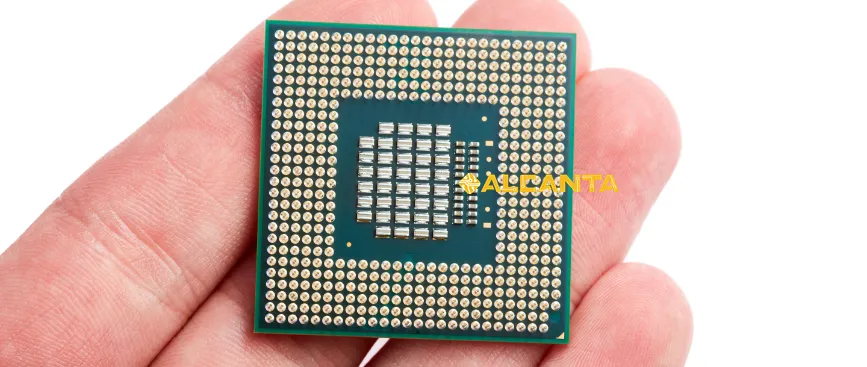
A glass substrate in the context of semiconductor packaging refers to a thin, flat piece of glass that serves as a foundation for mounting and interconnecting semiconductor components. It is typically made from materials such as borosilicate or aluminosilicate glass, known for their excellent thermal and chemical properties. Glass substrates provide a stable platform for integrating microelectronic devices and offer high electrical insulation, crucial for preventing short circuits and enhancing signal integrity in semiconductor applications.
Types of Glass Substrates Used in Semiconductor Packaging
1. Borosilicate Glass: Known for its low coefficient of thermal expansion (CTE), borosilicate glass is ideal for applications where thermal stability is critical. It is commonly used in microelectronics for its robustness and resistance to thermal shock.
2. Aluminosilicate Glass: This type of glass substrate offers enhanced mechanical strength and durability compared to borosilicate. Aluminosilicate glass is preferred in applications demanding higher levels of protection and reliability.
3. Specialty Glasses: Including compositions tailored for specific semiconductor packaging needs, such as glasses optimized for Through Glass Vias (TGVs) or for compatibility with advanced packaging techniques like System in Package (SiP).
Understanding these types of glass substrates is essential for selecting the most suitable material based on the application’s thermal, mechanical, and electrical requirements in semiconductor packaging.
Properties of Glass Substrates
Thermal Expansion Coefficient and Its Significance
The thermal expansion coefficient (CTE) of glass substrates plays a crucial role in semiconductor packaging. It refers to how much a material expands or contracts with changes in temperature. Glass substrates with low CTE are preferred because they minimize mechanical stress and potential cracking when exposed to temperature variations during manufacturing processes and operation. Borosilicate glass, for instance, has a CTE that closely matches that of silicon, making it suitable for applications where thermal compatibility is critical. This characteristic helps maintain the structural integrity of semiconductor devices and ensures reliable performance over time.
Electrical Properties and Insulation Capabilities
Glass substrates offer excellent electrical insulation, which is essential for preventing electrical shorts and interference between components in semiconductor devices. Their high dielectric strength and low electrical conductivity make them ideal for creating isolated pathways for electrical signals. This property enables the integration of complex circuitry and improves the overall reliability of electronic systems. Moreover, glass substrates can be engineered to have specific surface resistivity and capacitance characteristics, further enhancing their suitability for diverse semiconductor packaging applications.
Understanding these properties of glass substrates is essential for optimizing the design and performance of semiconductor packaging, ensuring robust functionality and longevity of electronic devices.
Applications of Glass Substrates in Semiconductor Packaging
Use in Through Glass Vias (TGVs) and Interposers
Glass substrates are increasingly utilized for Through Glass Vias (TGVs), which are vertical electrical interconnects passing through the thickness of the glass substrate. TGVs facilitate direct connections between different layers of semiconductor devices or between chips and packaging substrates without traditional wire bonding or flip-chip techniques. This technology enhances signal transmission efficiency, reduces signal loss, and allows for miniaturization by enabling high-density interconnects in compact electronic devices.
Interposers, which are used to connect multiple semiconductor chips within a single package, also benefit from glass substrates. The thermal stability and precise dimensional control of glass substrates ensure reliable alignment and connection of chips, supporting advanced packaging solutions.
Role in Advanced Packaging Technologies like System in Package (SiP)
Glass substrates play a critical role in System in Package (SiP) technologies, where multiple functional components such as microprocessors, memory, and sensors are integrated into a single package. Glass substrates enable the integration of diverse technologies onto a single substrate, providing thermal management, electrical insulation, and mechanical support. They facilitate the stacking and interconnection of chips or modules with different functions, optimizing space utilization and improving overall system performance and reliability.
In summary, glass substrates in semiconductor packaging enable innovative solutions like TGVs and SiP technologies, advancing the capabilities of electronic devices in terms of performance, compactness, and reliability. Their unique properties make them indispensable for modern semiconductor packaging applications.
Advantages of Glass Substrates
High Thermal Stability and Reliability
Glass substrates exhibit excellent thermal stability, which is critical in semiconductor packaging. They can withstand a wide range of operating temperatures without significant expansion or contraction, reducing the risk of mechanical stress on integrated circuits. This stability ensures consistent performance over time and under varying environmental conditions, enhancing the overall reliability of electronic devices. Borosilicate and aluminosilicate glasses, in particular, are known for their low coefficient of thermal expansion (CTE), closely matching that of semiconductor materials like silicon, thus minimizing thermal mismatch issues.
Compatibility with High-Density Integration and Miniaturization Trends
Glass substrates support high-density integration and miniaturization trends prevalent in modern semiconductor packaging. Their flat and smooth surfaces allow for precise patterning of conductive pathways and the integration of intricate circuitry. Glass substrates enable the creation of compact designs and facilitate the stacking of multiple layers or components in advanced packaging configurations such as System in Package (SiP) and 3D integration. This capability not only improves the performance of electronic devices by reducing signal propagation delays but also optimizes space utilization within devices, meeting the increasing demands for smaller, more efficient products.
In conclusion, the high thermal stability and compatibility with high-density integration make glass substrates a preferred choice in semiconductor packaging, contributing to the advancement of electronic technologies in terms of reliability, performance, and miniaturization.
Manufacturing Process of Glass Substrates
Overview of the Fabrication Methods
The manufacturing process of glass substrates for semiconductor packaging involves several critical steps to ensure precise dimensions, surface quality, and electrical properties:
1. Glass Selection: High-quality borosilicate or aluminosilicate glass is chosen based on desired thermal, mechanical, and electrical characteristics.
2. Cutting and Shaping: Glass sheets are cut into specific sizes and shapes using diamond saws or laser cutting methods to achieve precise dimensions.
3. Surface Polishing: The surfaces of glass substrates undergo polishing to achieve smoothness and flatness, essential for subsequent processing and ensuring proper adhesion of thin films and conductive layers.
4. Etching: Chemical etching processes are used to create Through Glass Vias (TGVs) or other microstructures on the glass substrate surface. This step involves precise control of etchant chemistry and duration to achieve desired feature sizes and depths.
5. Metallization: Thin films of metals such as copper, nickel, or gold are deposited onto the glass substrate surfaces using techniques like sputtering or electroplating. These metallization layers serve as conductive paths and bonding pads for semiconductor devices.
6. Annealing: Thermal annealing processes are employed to relieve residual stress in the glass substrate and metal layers, ensuring mechanical stability and enhancing overall reliability.
Quality Control and Testing Procedures
Quality control in glass substrate manufacturing is crucial to ensure consistency and reliability:
– Dimensional Measurement: Advanced metrology tools like optical profilometers and coordinate measuring machines (CMMs) are used to verify dimensional accuracy and tolerances of glass substrates.
– Surface Inspection: Automated inspection systems assess surface smoothness, defects (such as scratches or particles), and cleanliness, which are critical for ensuring proper functioning in semiconductor packaging.
– Electrical Testing: Electrical properties, including dielectric strength and insulation resistance, are evaluated to confirm that the glass substrates meet specifications for electrical performance.
– Thermal Cycling Tests: Glass substrates undergo thermal cycling tests to simulate operational conditions and verify their thermal stability and reliability over a range of temperatures.
– Adhesion and Bond Strength: Adhesion tests assess the strength of bonds between glass substrates and deposited thin films or adhesive materials used in packaging processes.
By implementing stringent quality control measures and testing procedures throughout the manufacturing process, manufacturers ensure that glass substrates meet the rigorous requirements of semiconductor packaging, contributing to the overall performance and reliability of electronic devices.
Case Studies and Examples
Success Stories from Semiconductor Companies Adopting Glass Substrates
1. Corning Inc.:Corning has been a prominent player in the development of specialty glass substrates for semiconductor packaging. Their advanced glass compositions, such as Corning® EAGLE XG® and Corning® Lotus™ NXT Glass, have been adopted by leading semiconductor manufacturers for their superior thermal stability and mechanical durability. These substrates enable the integration of TGVs and enhance the performance of microelectronic devices in terms of signal integrity and reliability.
2. AGC Inc.:AGC (Asahi Glass Co., Ltd.) has invested in the development of aluminosilicate glass substrates tailored for high-density integration and miniaturization trends in semiconductor packaging. Their glass substrates offer excellent electrical insulation and thermal management properties, supporting the implementation of SiP technologies. Semiconductor companies leveraging AGC’s glass substrates benefit from improved device performance and reduced form factor, meeting the demands of diverse applications from consumer electronics to automotive systems.
Performance Improvements and Cost-Effectiveness
– Signal Integrity Enhancement: Glass substrates contribute to improved signal transmission and reduced signal loss compared to traditional organic substrates. This enhancement is crucial for high-frequency applications in telecommunications, data centers, and automotive electronics.
– Thermal Management: The superior thermal stability of glass substrates helps dissipate heat efficiently, maintaining optimal operating conditions for semiconductor devices. This capability extends device lifespan and reliability, reducing maintenance costs and enhancing overall system performance.
– Miniaturization Benefits: By enabling high-density integration and stacking of components, glass substrates support the trend towards smaller and more compact electronic devices. This miniaturization not only saves space but also reduces material usage and assembly complexity, leading to cost savings in production.
– Long-Term Reliability: Semiconductor companies adopting glass substrates report improved long-term reliability due to reduced thermal expansion mismatches and better resistance to environmental stresses. This reliability translates into fewer failures and higher customer satisfaction, ultimately contributing to lower warranty and support costs.
These case studies and examples illustrate how semiconductor companies are leveraging the advantages of glass substrates to achieve significant performance improvements and cost-effectiveness in their packaging solutions. As the demand for smaller, faster, and more reliable electronic devices continues to grow, glass substrates play a pivotal role in meeting these evolving industry requirements.
FAQs about glass substrate for semiconductor packaging
The substrate material for semiconductors is typically silicon. Silicon wafers provide the foundation upon which semiconductor devices are fabricated. They offer excellent electrical properties, mechanical stability, and are compatible with the semiconductor manufacturing processes.
In the semiconductor industry, glasses such as borosilicate and aluminosilicate are commonly used. These glasses are chosen for their thermal stability, low coefficient of thermal expansion (CTE), and excellent electrical insulation properties. They are utilized in various applications including as substrates for packaging, creating Through Glass Vias (TGVs), and providing structural support for integrated circuits.
A glass substrate refers to a thin, flat piece of glass that serves as a base or foundation in various technological applications, including semiconductors. In the context of semiconductor packaging, glass substrates provide structural support, electrical insulation, and often include features like Through Glass Vias (TGVs) for interconnects between different layers or components.
Semiconductor chip packaging materials vary depending on the specific application and requirements. Common materials include ceramic, various types of plastics (such as epoxy resins), and metal alloys (like copper and aluminum). Each material offers different properties such as thermal conductivity, electrical insulation, mechanical strength, and compatibility with manufacturing processes, influencing their suitability for different packaging techniques and environments.

