
What Is a Substrate in Electronics: Key Types and Uses
In the realm of electronics, substrates serve as the silent heroes, providing the essential foundation upon which our devices operate. These often-overlooked components play a pivotal role in enabling the intricate functionality of semiconductor devices, intricate circuitry, and electronic boards that power our modern world. In this comprehensive exploration, we delve into the core of substrate technology, unraveling its significance and multifaceted applications across various domains. We’ll navigate through the substrates’ role in semiconductor manufacturing, circuit design, and electronic board construction, shedding light on their indispensable contribution to technological advancement. Through this journey, we’ll uncover the intricate structure and diverse applications of substrates, paving the way for a deeper understanding of their pivotal role in driving innovation in the electronics industry.
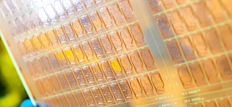
Substrate in Semiconductor: Building Blocks of Electronic Devices
A substrate in the context of semiconductors is a solid material upon which a semiconductor device is fabricated. It serves as the foundational layer onto which various semiconductor materials and components are deposited or grown. The substrate provides structural support, ensuring the stability and integrity of the intricate semiconductor layers that are essential for device functionality.
Substrates are crucial because they influence the electrical, thermal, and mechanical properties of the semiconductor device. By providing a base for epitaxial growth, substrates ensure that the semiconductor layers adhere properly and maintain their crystalline structure. This is vital for the performance of semiconductor devices, as any imperfections in the substrate can lead to defects in the semiconductor layers, adversely affecting the device’s efficiency and reliability.
Silicon is the most commonly used substrate material in semiconductor manufacturing. Its popularity stems from its excellent electronic properties, abundance, and the well-established infrastructure for silicon processing. Silicon substrates are used in the fabrication of a wide range of electronic components, including integrated circuits (ICs), microprocessors, and memory devices.
Silicon dioxide, another crucial substrate material, is often used as an insulating layer in semiconductor devices. It provides electrical insulation between different components and layers within a device, preventing unwanted electrical interference and enhancing overall performance. The use of silicon dioxide as a substrate material is particularly prevalent in metal-oxide-semiconductor (MOS) devices, which are foundational to modern electronics.
In summary, substrates in semiconductor manufacturing are fundamental to the creation of high-performance, reliable electronic devices. The choice of substrate material, such as silicon or silicon dioxide, plays a significant role in determining the device’s characteristics and capabilities. Understanding the importance of substrates and their materials is essential for advancing semiconductor technology and driving innovation in the electronics industry.
Exploring AMB and DBC Substrates
In the world of semiconductor device fabrication, AMB (Active Metal Brazed) and DBC (Direct Bond Copper) substrates are two prominent technologies used to enhance thermal and electrical performance. These substrates are essential in applications where high power and reliability are crucial, such as in power electronics and high-performance computing.
AMB (Active Metal Brazed) Substrates AMB substrates are created by brazing a metal, typically copper, onto a ceramic substrate using an active metal brazing process. This method involves the use of active metals like titanium, which facilitate the bonding of copper to ceramics at high temperatures. The ceramic base, often made of materials like aluminum nitride (AlN) or silicon nitride (Si3N4), provides excellent thermal conductivity and electrical insulation.
DBC (Direct Bond Copper) Substrates DBC substrates involve a process where copper foils are directly bonded to a ceramic substrate through a high-temperature oxidation process. The ceramic materials commonly used include aluminum oxide (Al2O3) and aluminum nitride (AlN). During the bonding process, an intermediate oxide layer forms, creating a strong bond between the copper and the ceramic substrate. This method ensures high thermal conductivity and mechanical stability.
Comparison of AMB and DBC Substrates
Characteristics:
- AMB Substrates:
- High thermal conductivity due to the use of ceramics like AlN or Si3N4.
- Strong mechanical bonding provided by the active metal brazing process.
- Excellent electrical insulation properties.
- DBC Substrates:
- High thermal conductivity, especially with AlN ceramics.
- Robust mechanical and thermal performance due to the direct bond process.
- Good electrical insulation provided by the ceramic base.
Applications:
- AMB Substrates:
- Power electronics such as IGBT (Insulated Gate Bipolar Transistor) modules.
- High-power LEDs.
- Automotive and aerospace applications where high reliability is required.
- DBC Substrates:
- Power modules for renewable energy systems.
- High-frequency and high-power semiconductor devices.
- Industrial and automotive applications requiring high thermal performance.
Manufacturing Processes:
- AMB:
- Involves active metal brazing, which requires precise control of temperature and environment to ensure strong bonding.
- Typically more complex and costly due to the need for active metals and high-temperature processing.
- DBC:
- Uses a high-temperature oxidation process to bond copper to the ceramic substrate.
- Generally more straightforward and cost-effective compared to AMB, with a well-established manufacturing process.
Advantages and Disadvantages
AMB Substrates:
- Advantages:
- Superior thermal conductivity due to advanced ceramic materials.
- Strong mechanical bonds, ideal for high-stress applications.
- Excellent electrical insulation.
- Disadvantages:
- Higher manufacturing costs due to the complex brazing process.
- Potential issues with thermal expansion mismatches between the metal and ceramic.
DBC Substrates:
- Advantages:
- High thermal conductivity and reliability.
- Cost-effective and established manufacturing process.
- Good thermal and mechanical performance.
- Disadvantages:
- Limited by the thermal expansion properties of the materials used.
- May not achieve the same level of thermal conductivity as some advanced AMB materials.
In summary, both AMB and DBC substrates offer unique benefits and are chosen based on specific application requirements in semiconductor device fabrication. Understanding their characteristics, applications, and manufacturing processes is crucial for selecting the appropriate substrate technology to meet the demands of modern electronic devices.
Electronic Substrates: The Backbone of Circuitry
Electronic substrates form the foundational layer upon which electronic circuits are built, playing a critical role in circuit design and construction. They provide the necessary support and electrical insulation for the components mounted on them, ensuring the reliable operation of electronic devices. These substrates must exhibit excellent mechanical strength, thermal stability, and electrical insulation properties to meet the demands of modern electronics.
Role in Circuit Design and Construction Electronic substrates serve several key functions in circuit design and construction:
- Mechanical Support: They provide a stable platform for mounting electronic components, preventing physical damage and ensuring structural integrity.
- Electrical Insulation: Substrates electrically isolate different components and conductive paths, preventing short circuits and interference.
- Thermal Management: They help dissipate heat generated by electronic components, maintaining optimal operating temperatures and preventing overheating.
- Interconnectivity: Substrates facilitate the connection of various components through conductive pathways, enabling the formation of complex electronic circuits.
Types of Electronic Substrates Several types of electronic substrates are commonly used in the industry, each with its unique properties and applications:
PCBs (Printed Circuit Boards)
- Materials: Typically made from fiberglass-reinforced epoxy resin (FR-4), PCBs can also use materials like polyimide for flexible circuits.
- Fabrication Process: Involves layering conductive copper tracks onto the substrate material through processes like etching, drilling, and plating.
- Applications: Widely used in consumer electronics, industrial equipment, automotive electronics, and more. They are the most common type of substrate due to their versatility and cost-effectiveness.
Ceramic Substrates
- Materials: Common ceramics used include aluminum oxide (Al2O3), aluminum nitride (AlN), and silicon nitride (Si3N4).
- Fabrication Process: Typically involves the deposition of metal layers onto ceramic substrates using techniques such as thick-film or thin-film deposition, followed by sintering or firing at high temperatures.
- Applications: Ideal for high-power and high-frequency applications due to their excellent thermal conductivity and electrical insulation. Used in power modules, RF components, and LED packaging.
Flexible Substrates
- Materials: Made from flexible materials like polyimide or polyethylene terephthalate (PET).
- Fabrication Process: Similar to rigid PCBs but designed to withstand bending and flexing, with conductive tracks printed or etched onto the flexible material.
- Applications: Used in wearable electronics, flexible displays, and other applications where flexibility and lightweight are essential.
Metal Core Substrates
- Materials: Consist of a metal core, usually aluminum or copper, sandwiched between layers of dielectric material.
- Fabrication Process: Involves bonding the metal core with dielectric layers and then applying conductive pathways through standard PCB fabrication techniques.
- Applications: Used in high-power applications where efficient heat dissipation is crucial, such as in LED lighting and power electronics.
Materials, Fabrication Processes, and Applications
Materials
- Epoxy Resins (FR-4): Commonly used for PCBs, offering a good balance of mechanical strength, electrical insulation, and cost-effectiveness.
- Polyimide: Used for flexible substrates, providing excellent thermal stability and flexibility.
- Ceramics (Al2O3, AlN, Si3N4): Used for ceramic substrates, offering superior thermal conductivity and electrical insulation.
- Metal Cores (Aluminum, Copper): Used in metal core substrates for high thermal conductivity and effective heat dissipation.
Fabrication Processes
- Etching: Used in PCB fabrication to create conductive pathways by removing unwanted copper.
- Deposition: Techniques like screen printing for thick-film or sputtering for thin-film deposition on ceramic substrates.
- Sintering/Firing: In ceramic substrate fabrication, involves heating the substrate to high temperatures to solidify the metal layers.
- Bonding: In flexible and metal core substrates, involves bonding different layers using adhesives or thermal processes.
Applications
- Consumer Electronics: PCBs are extensively used in smartphones, laptops, and home appliances.
- Automotive Electronics: Both PCBs and ceramic substrates are used in engine control units, sensors, and lighting systems.
- Power Electronics: Ceramic and metal core substrates are used in power modules, inverters, and LED drivers.
- Medical Devices: Flexible substrates are used in wearable medical devices and diagnostic equipment.
In summary, electronic substrates are the backbone of modern electronic circuits, providing essential support, insulation, and thermal management. Understanding the different types of substrates, their materials, fabrication processes, and applications is crucial for designing and manufacturing reliable, high-performance electronic devices.
Substrates in Circuits: Enabling Connectivity and Functionality
Importance of Substrates in Circuitry
Substrates are fundamental to the functionality and reliability of electronic circuits. They provide the necessary support structure for mounting electronic components and play a crucial role in maintaining the integrity of electrical connections. Without substrates, it would be impossible to achieve the compact and intricate layouts required for modern electronic devices. Substrates not only offer mechanical support but also ensure electrical isolation and efficient heat dissipation, which are essential for the proper operation and longevity of electronic circuits.
Facilitating Interconnection and Enabling Functionality
Substrates facilitate the interconnection of electronic components through the following mechanisms:
- Conductive Pathways: Substrates are embedded with conductive traces, usually made of copper, which form the electrical pathways connecting various components on the circuit. These traces are meticulously designed to ensure optimal signal transmission and minimize interference.
- Component Mounting: Substrates provide a stable platform for soldering and mounting components, such as resistors, capacitors, and integrated circuits. This ensures that components remain securely in place during the device’s operation and handling.
- Electrical Insulation: Substrates are made of insulating materials that prevent electrical shorts and cross-talk between adjacent conductive traces and components. This insulation is critical for maintaining the circuit’s intended functionality.
- Thermal Management: Efficient heat dissipation is facilitated by the substrate material, preventing overheating and ensuring that components operate within their specified temperature ranges. This is particularly important in high-power applications.
Types of Substrates Used in Circuit Manufacturing
FR-4 Substrates
- Materials: FR-4 is a composite material made from woven fiberglass cloth with an epoxy resin binder. It is the most widely used substrate material for printed circuit boards (PCBs).
- Fabrication Process: The manufacturing process involves layering copper foil on both sides of the FR-4 laminate, followed by etching to create the desired circuit patterns. Drilling and plating are used to form vias that connect different layers of the board.
- Applications: FR-4 substrates are commonly used in consumer electronics, telecommunications, automotive electronics, and industrial control systems due to their excellent mechanical strength, electrical insulation properties, and cost-effectiveness.
Flexible Substrates
- Materials: Flexible substrates are typically made from polyimide or polyester films, which provide flexibility and durability.
- Fabrication Process: Similar to rigid PCBs, but designed to withstand bending and flexing. Conductive traces are printed or etched onto the flexible material, and components are mounted using surface-mount technology.
- Applications: Flexible substrates are used in applications where space constraints and flexibility are critical, such as wearable electronics, flexible displays, medical devices, and compact consumer electronics.
Metal Core Substrates
- Materials: These substrates consist of a metal core, usually aluminum or copper, sandwiched between layers of dielectric material.
- Fabrication Process: The metal core is bonded with dielectric layers, and then copper traces are applied using standard PCB fabrication techniques. The metal core acts as a heat sink, effectively dissipating heat generated by electronic components.
- Applications: Metal core substrates are used in high-power and high-heat applications, such as LED lighting, power electronics, and automotive applications where efficient thermal management is crucial.
Ceramic Substrates
- Materials: Common ceramic materials include aluminum oxide (Al2O3), aluminum nitride (AlN), and silicon nitride (Si3N4).
- Fabrication Process: The process typically involves the deposition of metal layers onto ceramic substrates using thick-film or thin-film techniques, followed by high-temperature sintering or firing.
- Applications: Ceramic substrates are preferred in high-frequency and high-power applications due to their excellent thermal conductivity and electrical insulation properties. They are used in RF components, power modules, and LED packaging.
Substrates are indispensable in circuitry, providing the necessary foundation for mounting components, ensuring electrical connectivity, and managing heat dissipation. Different types of substrates, such as FR-4, flexible substrates, metal core substrates, and ceramic substrates, offer unique advantages and are chosen based on the specific requirements of the application. Understanding the properties and fabrication processes of these substrates is essential for designing reliable, high-performance electronic circuits.
Future Trends and Developments in Substrate Technology
As the electronics industry continues to evolve at a rapid pace, substrate technology is experiencing significant advancements and emerging trends that promise to revolutionize the way electronic devices are designed, manufactured, and utilized. These innovations are driven by the need for higher performance, miniaturization, energy efficiency, and the integration of new functionalities.
Emerging Trends and Advancements
Advanced Materials
- Graphene and 2D Materials: Graphene, with its exceptional electrical, thermal, and mechanical properties, is being explored as a potential substrate material. Other two-dimensional (2D) materials, such as molybdenum disulfide (MoS2) and hexagonal boron nitride (h-BN), are also under investigation for their unique properties that can enhance electronic performance.
- High-Performance Ceramics: Advancements in ceramic materials, such as silicon carbide (SiC) and gallium nitride (GaN), offer superior thermal conductivity and electrical insulation. These materials are particularly beneficial in high-power and high-frequency applications.
Flexible and Stretchable Substrates
- Organic Electronics: Organic materials, including conductive polymers and small molecules, are being developed for use in flexible and stretchable substrates. These materials enable the creation of foldable displays, wearable electronics, and other flexible devices.
- Nanomaterials: Incorporating nanomaterials like carbon nanotubes and nanowires into flexible substrates enhances their electrical and mechanical properties, paving the way for next-generation flexible electronics.
Advanced Manufacturing Processes
- 3D Printing: Additive manufacturing techniques, such as 3D printing, are being adapted for substrate fabrication. This allows for the creation of complex geometries and multi-material substrates with tailored properties, enabling new design possibilities.
- Roll-to-Roll Processing: For flexible and large-area electronics, roll-to-roll processing offers a cost-effective and scalable manufacturing method. This technique enables the continuous production of flexible substrates with high throughput.
- Microfabrication Techniques: Advances in microfabrication, including photolithography and etching, are enhancing the precision and complexity of substrate designs. These techniques support the miniaturization and integration of more components on a single substrate.
Predicting Future Developments
Substrate Materials
- Hybrid Materials: The development of hybrid substrates that combine the best properties of different materials, such as ceramics with polymers or metals with graphene, will lead to substrates with superior performance and versatility.
- Biocompatible Materials: In the realm of medical electronics and wearables, biocompatible substrates that can safely interact with biological tissues will become increasingly important. Materials like silk, cellulose, and certain biodegradable polymers are being researched for these applications.
Manufacturing Processes
- Nanoimprint Lithography: This advanced lithography technique allows for the patterning of nanoscale features on substrates, enabling the fabrication of highly integrated and miniaturized electronic circuits.
- Self-Assembly Techniques: Utilizing self-assembly processes at the molecular level can lead to the creation of highly ordered and functional substrate structures, enhancing their electrical and thermal properties.
Applications
- Internet of Things (IoT): Substrate innovations will drive the proliferation of IoT devices, which require compact, energy-efficient, and highly reliable substrates to connect and communicate seamlessly.
- Wearable Technology: The development of flexible and stretchable substrates will enable more sophisticated and comfortable wearable devices, with applications ranging from health monitoring to augmented reality.
- Energy Harvesting: Advanced substrates will play a crucial role in energy harvesting technologies, such as flexible solar panels and thermoelectric generators, providing sustainable power solutions for a variety of applications.
Potential Impact on the Electronics Industry and Society
Enhanced Performance and Miniaturization
Innovations in substrate technology will lead to electronic devices that are smaller, faster, and more efficient. This will enable the continued miniaturization of devices, making powerful computing and connectivity available in even the most compact form factors.
Sustainability and Energy Efficiency
Advanced substrates that improve thermal management and reduce power consumption will contribute to the development of greener electronics. This will support global efforts to reduce energy usage and mitigate the environmental impact of electronic devices.
Medical and Health Applications
The integration of biocompatible and flexible substrates in medical devices will revolutionize healthcare, enabling more effective diagnostics, monitoring, and treatment options. Wearable health monitors, implantable devices, and smart medical sensors will enhance patient care and improve health outcomes.
Economic Growth and Innovation
The advancements in substrate technology will spur economic growth by driving innovation across various sectors, including consumer electronics, automotive, healthcare, and telecommunications. This will create new market opportunities, stimulate investment, and generate high-tech jobs.
The future of substrate technology is poised to bring transformative changes to the electronics industry and society. By leveraging advanced materials, innovative manufacturing processes, and new applications, substrate innovations will enhance device performance, support sustainable development, and improve quality of life across the globe.
FAQs About what is a substrate in electronics
A substrate in a semiconductor refers to the base material, typically silicon, onto which semiconductor devices and circuits are fabricated. It provides the necessary structural support and electrical properties required for the growth of semiconductor layers and the integration of electronic components.
An electronic substrate is a foundational material used in the construction of electronic circuits and devices. It serves as a physical support for electronic components and provides electrical insulation and thermal management. Common materials for electronic substrates include FR-4 (fiberglass epoxy), ceramics, and flexible polymers.
In circuits, a substrate is the underlying material on which electrical components and conductive pathways are mounted and connected. It ensures mechanical stability, electrical isolation, and thermal dissipation, allowing the circuit to function reliably and efficiently. Substrates in circuits include printed circuit boards (PCBs) made of FR-4, flexible substrates, and metal core substrates.
Substrates in technology refer to the base materials used across various fields to support and integrate different components and systems. In electronics, they are essential for mounting and connecting electronic components. Substrates are also used in other technologies such as photovoltaics, LEDs, and MEMS (micro-electromechanical systems), playing a crucial role in the functionality and performance of these devices.

