
Driving Innovation: Glass Substrates in Semiconductor Technology
The semiconductor industry is marked by relentless progress and mounting challenges as devices become smaller, faster, and more efficient. This evolution demands innovations in all components, especially substrates—the foundational material layer upon which devices are built. Traditional substrates, primarily silicon-based, are approaching physical and performance limits, especially in thermal management and feature scaling. As these challenges escalate, the industry is increasingly turning towards alternative materials that can surpass these limitations. Enter glass substrates, a revolutionary option characterized by superior flatness, thermal stability, and electrical insulation properties. The emergence of glass substrates not only promises to overcome the drawbacks of traditional materials but also opens up new avenues in semiconductor design and functionality, highlighting their potential to reshape the future of semiconductor manufacturing.
Overview of Glass Substrate
What are Glass Substrates?
Glass substrates refer to thin sheets of specially processed glass that serve as a foundational layer in various electronic and optical applications. Unlike traditional substrates that often utilize silicon or ceramics, glass substrates are chosen for their unique properties such as transparency, electrical insulation, thermal stability, and smooth surface quality. These characteristics make them particularly advantageous for applications such as advanced display technologies, semiconductor packaging, and high-frequency electronics.
History and Development Background of Glass Substrates
The development of glass substrates is a response to the increasing demands for more sophisticated electronics. Historically, substrates were dominated by materials like silicon and gallium arsenide, which provided the necessary electrical characteristics but often fell short in terms of thermal management and integration density. The introduction of glass as a substrate material began as a niche application in the display industry, particularly with the advent of LCD technology in the late 20th century. Since then, advancements in glass composition and manufacturing techniques have expanded its use into broader semiconductor and optoelectronic applications, spurred by the need for higher performance and greater integration of electronic components.
Introduction to Major Manufacturers
Two of the leading manufacturers in the glass substrate industry are Intel and AGC (Asahi Glass Co.). Intel, traditionally known for its semiconductor products, has been at the forefront of integrating glass substrates into more complex semiconductor packaging solutions. Their work has helped demonstrate the feasibility of using glass for high-density, high-performance chips, positioning glass substrates as a viable alternative to conventional materials in microelectronics.
AGC, on the other hand, has leveraged its expertise in glass manufacturing to produce high-quality glass substrates that are used not only in semiconductors but also in a variety of display technologies. Their products are renowned for their high transparency and superior mechanical properties, making them ideal for sensitive applications such as smartphones, tablets, and other consumer electronics.
Together, these companies are driving the evolution of glass substrates, continuously improving the material properties and production techniques to meet the industry’s growing demands.
Technical Advantages of Glass Substrates
High Flatness and Low Coefficient of Thermal Expansion
One of the critical advantages of glass substrates is their exceptionally high flatness, which is crucial for the uniformity and precision required in advanced semiconductor processes and high-resolution display manufacturing. The surface irregularities are minimized to a few nanometers, allowing for more consistent layering and higher device performance. Additionally, glass substrates exhibit a low coefficient of thermal expansion (CTE), meaning they expand and contract very little with temperature changes. This property is essential for maintaining structural integrity and operational reliability under varying thermal conditions, which is particularly valuable in environments subject to rapid temperature fluctuations.
Better Electrical Insulation Properties
Glass substrates provide superior electrical insulation compared to traditional semiconductor substrates. This characteristic is especially beneficial in high-density chip designs where leakage currents and cross-talk between circuits can significantly degrade performance. The insulating properties of glass help in isolating electrical components at micro and nano scales, thus enhancing the overall efficiency and performance of electronic devices. This advantage makes glass substrates ideal for use in complex, multi-layered electronic architectures that are common in modern consumer electronics and communication devices.
High Transparency and Excellent Optical Performance
The inherent transparency of glass substrates is a significant advantage in applications requiring light transmission, such as sensors, imaging devices, and particularly in display technologies. This optical clarity supports improved image quality and color fidelity in LCDs, OLEDs, and other display types. Moreover, glass substrates can be engineered to enhance specific optical properties, such as anti-reflective coatings or improved light-guiding capabilities, to further boost the performance of optical systems.
Mechanical Strength and Chemical Stability
Despite their transparency and excellent optical qualities, glass substrates are mechanically robust and offer significant resistance to physical stress and chemical attack. This strength ensures durability and a longer lifespan for devices, particularly important in mobile devices that are frequently exposed to mechanical stress. Chemical stability, another critical feature, means that glass substrates can withstand harsh environments and aggressive chemical agents used during device fabrication and operation, which helps in maintaining the integrity and performance of the device over time.
The combination of these technical advantages makes glass substrates a highly desirable material in a wide range of semiconductor and optical applications, pushing the boundaries of what is achievable with traditional materials.
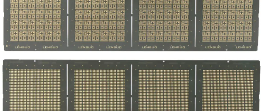
Applications of Glass Substrates in Semiconductors
Integrated Circuit (IC) Packaging
Glass substrates are increasingly used in the packaging of integrated circuits (ICs) due to their exceptional thermal stability and electrical insulation properties. These characteristics are critical in high-density ICs where heat dissipation and electrical isolation are paramount for performance and reliability. Glass substrates allow for the development of thinner, lighter, and more robust IC packages that can withstand the thermal and mechanical stresses encountered in high-performance computing and consumer electronics. This application has become particularly significant in the context of semiconductor miniaturization trends such as system-on-chip (SoC) and package-on-package (PoP) technologies.
Display Technologies (such as OLED and LCD)
In the realm of display technologies, glass substrates play a pivotal role, especially in OLED (Organic Light Emitting Diode) and LCD (Liquid Crystal Display) screens. The high transparency and excellent optical properties of glass ensure clear, vibrant displays with high color fidelity. Moreover, the smooth and flat surface of glass substrates is essential for the uniform deposition of organic and liquid crystal materials, which directly impacts the quality and performance of the display. Glass substrates also contribute to the overall durability and scratch resistance of the screen, enhancing the product’s lifespan and user experience.
Sensors and MEMS Devices
Glass substrates are instrumental in the production of sensors and micro-electromechanical systems (MEMS). These devices often require precise dimensional stability and excellent insulating properties, which glass substrates provide. Applications range from automotive sensors, environmental monitoring devices to biomedical implants. The chemical stability and biocompatibility of glass make it suitable for sensitive applications such as medical diagnostics and implantable devices, where other materials might fail or induce adverse reactions.
5G and Optical Communication Fields
The advent of 5G technology and the expansion of optical communication infrastructures have created a demand for materials that can support higher frequencies and improved signal integrity. Glass substrates are ideal for these applications due to their low dielectric constant and loss tangent, which minimize signal loss and cross-talk at high frequencies. This makes them suitable for use in optical transceivers, waveguides, and other components critical to the efficient and reliable transmission of data over vast distances. Additionally, the ability of glass to be precision-molded at micro and nano scales allows for the integration of optical functions directly onto the substrate, paving the way for more compact and less expensive communication devices.
These diverse applications underscore the versatility and critical role of glass substrates in pushing the frontiers of semiconductor technology and enabling the next generation of electronic and optical devices.
Intel’s Glass Substrate Technology
Innovations in Intel’s Glass Substrate Technology
Intel has been at the forefront of incorporating glass substrates into semiconductor technology, driving innovation with its unique approaches to overcoming traditional limitations in IC packaging and system integration. Intel’s research and development have focused on enhancing the electrical performance and thermal management capabilities of glass substrates, which are critical for high-performance computing and densely packed ICs. One notable innovation includes the development of proprietary glass materials that offer enhanced thermal conductivity while maintaining excellent electrical insulation. Intel has also pioneered techniques for embedding active and passive components directly into the glass substrates, a process that significantly reduces package size and improves signal integrity, leading to faster and more efficient devices.
Relevant Technical Documents and PDF Resources
Intel provides a wealth of technical documents and resources that detail their advancements in glass substrate technology. These documents often include white papers, research findings, and technical specifications that are accessible via Intel’s official website or through scholarly and industry publications. For those interested in the technical aspects and the scientific foundation behind these innovations, Intel’s technical PDFs serve as a valuable resource. They cover topics from the basic properties of their glass substrates to complex case studies demonstrating their application in real-world scenarios.
Real-world Application Cases and Success Stories
Intel’s glass substrate technology has been applied across various domains, demonstrating significant benefits in terms of device performance and reliability. One of the prominent success stories is its use in high-performance processors where glass substrates have enabled thinner, lighter designs without compromising the heat handling capabilities required for intense computing tasks. Another significant application has been in the development of wearables and mobile devices, where the reduced form factor and improved thermal characteristics of glass substrates have allowed for sleeker designs with extended battery life and enhanced functionality. Intel’s collaborations with automotive and aerospace industries also highlight the impact of their glass substrates in harsh environments where durability and precise performance are paramount.
Through these innovations and applications, Intel’s glass substrate technology not only showcases its versatility but also sets a benchmark in the semiconductor industry, indicating a shift towards more integrated and efficient electronic devices.
AGC Glass Substrate Products
Features of AGC Glass Substrates
AGC (Asahi Glass Co.) has developed glass substrates that are renowned for their superior quality and advanced features tailored to meet the demands of various high-tech industries. Key features of AGC glass substrates include exceptional flatness and smoothness, which are critical for precise deposition of materials in semiconductor manufacturing and high-resolution display production. Additionally, AGC glass substrates boast a high degree of transparency and optical clarity, making them ideal for applications in the display sector. Their substrates are also designed to have a low coefficient of thermal expansion and high thermal resistance, ensuring stability and reliability under operational stresses such as temperature fluctuations and physical impacts.
Product Lines and Their Application Areas
AGC offers a diverse range of glass substrate products, each tailored for specific applications. For instance, their line of ultra-thin glass substrates is designed for the burgeoning market of flexible electronics, including flexible displays and wearable technology. AGC also produces specialized glass substrates for use in OLED and LCD displays, highlighting their role in enhancing the performance and durability of modern display technologies. Beyond displays, AGC’s substrates are integral to photovoltaic panels and semiconductor packaging, where their chemical resistance and mechanical strength are vital for long-term performance and reliability.
Market Response and User Feedback
The market response to AGC’s glass substrates has been overwhelmingly positive, with customers praising the quality and performance of their products. User feedback often highlights the reliability and enhanced capabilities that AGC glass substrates bring to electronic and optical components, particularly noting improvements in device lifespan and operational efficiency. In the display industry, for example, manufacturers have acknowledged that switching to AGC’s high-performance glass substrates has resulted in clearer, more vibrant displays with higher durability. Similarly, in the semiconductor sector, feedback has emphasized the substrates’ ability to support more complex, higher-density circuit designs, which are crucial for advancing miniaturization and integration trends in electronics.
AGC’s commitment to innovation and quality in its glass substrate products has not only captured a substantial market share but also established the company as a leader in the substrate technology sector, continuously pushing the boundaries of what glass can achieve in high-tech applications.
Comparison with Traditional Substrates
Performance Comparison Between Silicon and Glass Substrates
Silicon has long been the standard substrate in semiconductor manufacturing due to its excellent electrical properties and compatibility with semiconductor processes. However, glass substrates are emerging as a compelling alternative, especially in applications requiring superior optical performance and improved thermal stability. Glass substrates offer higher transparency, which is crucial for optical applications such as sensors and display technologies. They also exhibit lower thermal expansion rates compared to silicon, which makes them more stable under thermal stress and thus more reliable over a range of operating temperatures. On the other hand, silicon substrates generally provide better electrical performance for high-frequency applications, making them more suitable in areas where electrical properties are prioritized over thermal and optical considerations.
Analysis of Advantages and Disadvantages Compared to Ceramic Substrates
Ceramic substrates are known for their high thermal conductivity and mechanical strength, making them ideal for high-power electronic applications where heat dissipation is critical. However, glass substrates have a distinct advantage in terms of cost-effectiveness and manufacturability. They can be produced with greater dimensional uniformity and at lower temperatures, reducing manufacturing costs and complexity. Glass also typically offers better insulation properties and is less brittle compared to ceramic, which enhances durability and reduces the risk of damage during handling and operation. The main disadvantage of glass compared to ceramics is its lower thermal conductivity, which may limit its use in applications where rapid heat dissipation is essential.
Comprehensive Cost-Benefit Analysis
From a cost-benefit perspective, glass substrates provide a competitive edge in many applications. The lower material and production costs of glass make it an economically attractive option, especially for large-scale and high-volume manufacturing settings. The ability to integrate multiple functions onto a single glass substrate can further reduce the overall cost of materials and streamline production processes. However, it is important to consider the total lifecycle costs, including durability and maintenance. Glass substrates typically offer longer lifespans and less frequent need for replacements due to their chemical stability and mechanical strength, contributing to lower total ownership costs. When evaluating the cost-effectiveness of glass versus traditional substrates like silicon and ceramic, factors such as application-specific requirements, environmental stability, and future scalability must also be taken into account to make an informed decision.
This comprehensive analysis underscores the situational advantages and considerations when choosing between glass, silicon, and ceramic substrates, highlighting the importance of aligning substrate selection with specific application needs and performance requirements.
FAQs about glass substrate for semiconductor
The substrate material for semiconductors can vary, but commonly used materials include silicon, germanium, and gallium arsenide. Silicon is the most widely used due to its excellent semiconductor properties and abundance.
Glass substrates are sheets of glass used as the base layer upon which devices such as semiconductors, LCD displays, and solar cells are built. These substrates are chosen for their optical transparency, chemical stability, and flat surfaces.
Yes, glass can be used as a substrate in various applications. It is particularly valued in fields requiring high optical clarity and stability, such as in display technology (LCDs, OLEDs) and some types of semiconductor packaging.
In semiconductor packaging, a substrate refers to the base material upon which semiconductor devices or integrated circuits are mounted. The substrate helps to support the semiconductor device and facilitates electrical connections between the chip and the external environment. It can be made from materials like silicon, ceramic, or advanced polymers and, increasingly, glass.

