
DNP Glass Substrate: Precision for High-Tech Evolution
Dai Nippon Printing Co., Ltd. (DNP) is a global leader in printing and information technology, renowned for its innovative contributions to various industries, including electronics. Established in 1876, DNP has consistently pioneered advancements in materials science, particularly in the development of high-performance glass substrates.
Glass substrates have become crucial in the modern electronics industry due to their exceptional thermal stability, precision, and optical clarity. These properties make them indispensable for applications in semiconductors, displays, and other high-tech fields, where traditional materials like silicon fall short.
This article aims to provide a comprehensive overview of DNP glass substrates, highlighting their unique characteristics, diverse applications, and the advantages they offer over other materials. By delving into the technical aspects and real-world uses of DNP’s glass substrates, we will illustrate how DNP continues to drive innovation and excellence in the electronics industry.
What is DNP Glass Substrate?
Definition and Basic Concepts
DNP glass substrates are high-performance glass materials engineered for use in advanced electronic applications. These substrates are known for their superior properties, including high precision, thermal stability, and optical clarity. They serve as foundational components in the manufacturing of semiconductors, displays, and other electronic devices, offering a reliable alternative to traditional silicon substrates.
DNP’s Role and Historical Background in the Glass Substrate Field
DNP (Dai Nippon Printing Co., Ltd.) has a storied history in the development and production of high-quality glass substrates. Founded in 1876, DNP initially focused on printing and information technology but gradually expanded its expertise into materials science and electronics. Over the decades, DNP has become a leader in the innovation and commercialization of glass substrates, leveraging its extensive research and development capabilities to address the evolving needs of the electronics industry.
Introduction to Dai Nippon Printing Co., Ltd. (DNP)
Dai Nippon Printing Co., Ltd., commonly known as DNP, is one of Japan’s largest printing companies, with a diverse portfolio that spans multiple industries, including electronics, packaging, and information technology. With a commitment to innovation and sustainability, DNP has continuously pushed the boundaries of what is possible in materials science and engineering.
DNP’s Innovations in Materials Science and the Electronics Industry
DNP’s foray into the electronics industry has been marked by significant technological advancements. The company has developed proprietary processes and technologies that enhance the performance of glass substrates. For instance, DNP has pioneered methods to achieve ultra-high flatness and minimal thermal expansion in glass materials, making them ideal for precise electronic applications. Their glass substrates are designed to withstand high temperatures and mechanical stresses, ensuring reliability and performance in demanding environments.
DNP’s innovations extend beyond product development to include advancements in manufacturing processes. The company utilizes state-of-the-art facilities and automated production lines to ensure consistent quality and scalability. This has enabled DNP to meet the growing demand for high-performance glass substrates in various applications, from consumer electronics to industrial systems.
DNP glass substrates represent the culmination of over a century of expertise and innovation in materials science. By continuously improving the properties and manufacturing processes of these substrates, DNP has solidified its position as a key player in the electronics industry, driving progress and enabling the development of next-generation electronic devices.
Characteristics of DNP Glass Substrate
Key Features
DNP glass substrates are designed to meet the rigorous demands of modern electronic applications. They are engineered with precision to offer a range of superior properties that make them ideal for use in various high-tech industries. These key features include high precision and flatness, excellent thermal stability, low thermal expansion coefficient, and exceptional transparency and optical performance. These characteristics ensure that DNP glass substrates provide reliable and high-quality performance in advanced electronic devices.
High Precision and Flatness
One of the standout features of DNP glass substrates is their high precision and flatness. Achieving a high degree of flatness is crucial for applications such as semiconductor manufacturing, where even the smallest deviations can lead to significant performance issues. DNP utilizes advanced manufacturing techniques to ensure that their glass substrates maintain an extremely flat surface, with minimal deviations. This precision is essential for creating intricate electronic circuits and components, allowing for greater accuracy and reliability in the final products.
Excellent Thermal Stability
Thermal stability is another critical characteristic of DNP glass substrates. In many electronic applications, substrates are subjected to high temperatures during manufacturing processes such as soldering or during operation in high-performance computing environments. DNP glass substrates are designed to withstand these high temperatures without deforming or losing their structural integrity. This excellent thermal stability ensures that the substrates maintain their performance characteristics, even under demanding thermal conditions, contributing to the overall reliability and longevity of electronic devices.
Low Thermal Expansion Coefficient
The low thermal expansion coefficient of DNP glass substrates further enhances their suitability for electronic applications. Materials with low thermal expansion coefficients expand and contract less with temperature changes, reducing the risk of mechanical stress and potential damage. This property is particularly important in multilayer electronic assemblies, where different materials must work together without causing stress or misalignment. DNP’s glass substrates maintain dimensional stability across a wide range of temperatures, ensuring consistent performance and reducing the likelihood of thermal-induced failures.
Transparency and Optical Performance
Transparency and optical performance are vital for applications such as displays and optical devices. DNP glass substrates offer exceptional optical clarity, allowing for high-quality light transmission and minimal distortion. This makes them ideal for use in high-resolution displays, optical sensors, and other applications where clarity and precision are paramount. The substrates’ transparency ensures that they do not interfere with the functionality of optical components, thereby enhancing the overall performance of the device.
Technical Parameters and Specifications
DNP glass substrates are available in various specifications to meet the diverse needs of different applications. Typical technical parameters include:
- Thickness: Ranging from ultra-thin options for flexible electronics to thicker substrates for robust applications.
- Size: Customizable to fit specific device requirements, from small sensor components to large display panels.
- Flatness: Achieving flatness levels within microns, crucial for high-precision applications.
- Surface Roughness: Low surface roughness to ensure smooth interfaces with other materials and components.
- Thermal Expansion Coefficient: Typically in the range of 0.5 to 1.0 x 10^-6/°C, ensuring minimal expansion and contraction.
- Optical Properties: High transmission rates across various wavelengths, low refractive index variations, and minimal birefringence.
These technical parameters are meticulously controlled and optimized to ensure that DNP glass substrates meet the highest standards of quality and performance. By offering a range of customizable options, DNP can provide tailored solutions for specific industry needs, enhancing the functionality and efficiency of electronic devices across various sectors.
In summary, the characteristics of DNP glass substrates make them an excellent choice for a wide range of high-tech applications. Their high precision and flatness, excellent thermal stability, low thermal expansion coefficient, and superior transparency and optical performance ensure that they deliver reliable, high-quality performance in demanding electronic environments.
Applications of DNP Glass Substrate
Electronics and Semiconductor Industry
CPU and GPU Substrates
DNP glass substrates play a crucial role in the manufacturing of CPUs (Central Processing Units) and GPUs (Graphics Processing Units). These components are the heart of computing devices, requiring substrates that offer high precision and excellent thermal management. The superior thermal stability and low thermal expansion coefficient of DNP glass substrates ensure that CPUs and GPUs can operate efficiently under high temperatures and heavy workloads. Additionally, the flatness and precision of these substrates enable the intricate wiring and microfabrication processes needed to create these advanced semiconductor devices, leading to enhanced performance and reliability.
Glass Core Substrates
Glass core substrates are increasingly being used in the semiconductor industry due to their exceptional electrical insulation properties and mechanical stability. DNP’s glass core substrates provide a robust platform for embedding fine circuit patterns, which is essential for miniaturization in advanced electronic devices. These substrates are ideal for multi-chip modules and high-density interconnects, supporting the trend towards smaller, more powerful electronic devices. The high precision and flatness of DNP glass core substrates also facilitate better alignment and bonding of multiple layers, improving overall device performance.
Glass Interposers
Glass interposers are used in advanced packaging technologies to connect different semiconductor components within a single package. DNP’s glass interposers offer superior electrical performance, low signal loss, and high-frequency capabilities, making them ideal for applications such as 2.5D and 3D IC packaging. These interposers provide a stable and reliable platform for high-speed signal transmission, essential for modern computing and communication devices. The transparency and optical properties of DNP glass interposers also allow for advanced optical communication applications, further extending their versatility in the semiconductor industry.
Display Technologies
High-Resolution Displays
DNP glass substrates are fundamental in the production of high-resolution displays, such as those used in smartphones, tablets, and high-definition televisions. The substrates’ optical clarity and smooth surface are critical for ensuring that the displays can produce sharp, vibrant images with high color accuracy. The excellent thermal stability of DNP glass substrates also helps maintain display performance under various environmental conditions, ensuring consistent image quality and longevity.
OLED and LCD Panels
Organic Light Emitting Diode (OLED) and Liquid Crystal Display (LCD) panels rely on high-quality substrates to achieve their superior display characteristics. DNP glass substrates provide the necessary transparency and smooth surface required for these technologies. In OLED panels, the substrates support the thin film layers that emit light, contributing to the display’s overall brightness and efficiency. For LCD panels, the glass substrates provide a stable base for the liquid crystals and the electrodes that control pixel activation, ensuring precise image rendering and fast response times.
Other High-Tech Fields
Sensors
In the field of sensors, DNP glass substrates are used to create highly sensitive and accurate sensing devices. These substrates’ low thermal expansion coefficient and excellent thermal stability ensure that the sensors can operate reliably in various temperature conditions. Additionally, the optical clarity of DNP glass substrates is crucial for optical sensors, enabling precise detection and measurement of light, which is essential for applications in medical diagnostics, environmental monitoring, and industrial automation.
Optical Components
DNP glass substrates are also integral to the production of various optical components, such as lenses, mirrors, and prisms. The high optical performance and transparency of these substrates make them ideal for applications requiring precise light manipulation and transmission. This includes advanced optical systems in telecommunications, laser technologies, and scientific instrumentation. The precision and flatness of DNP glass substrates ensure minimal distortion and high fidelity in optical applications, contributing to the development of high-performance optical devices.
In summary, DNP glass substrates are indispensable across multiple high-tech fields, thanks to their superior properties and performance. From enhancing the capabilities of CPUs and GPUs to supporting the latest advancements in display technologies and sensors, these substrates are at the forefront of innovation in the electronics and semiconductor industries. Their versatility and reliability make them a critical component in the ongoing development of advanced electronic and optical devices.
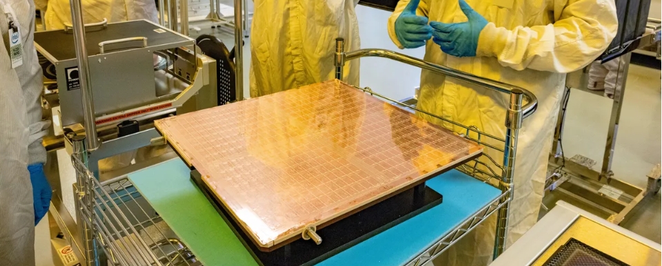
Manufacturing Process of DNP Glass Substrate
Manufacturing Process
The manufacturing process of DNP glass substrates is a meticulous and technologically advanced procedure that ensures the highest quality and performance. This process involves several critical stages, from material selection to the final precision machining and surface treatment. Each step is designed to maximize the substrates’ physical and chemical properties, making them suitable for a wide range of high-tech applications.
Material Selection
The foundation of a high-quality glass substrate lies in the selection of raw materials. DNP employs stringent criteria to choose the best raw materials, focusing on purity, consistency, and performance characteristics. The selected glass must possess excellent thermal and mechanical properties, such as low thermal expansion, high thermal stability, and superior optical clarity. DNP sources these materials from reputable suppliers to ensure that the substrates meet the exacting standards required for advanced electronic and optical applications.
Cutting and Shaping
Once the raw materials are selected, the next step is cutting and shaping the glass to the desired dimensions. DNP uses advanced cutting technologies, such as laser cutting and precision sawing, to achieve the required shapes and sizes with high accuracy. This stage is crucial for ensuring that the glass substrates fit perfectly into their intended applications, whether they are used in semiconductor devices, displays, or optical components. The precision in cutting and shaping also helps minimize material waste and ensures uniformity across batches.
Precision Machining and Surface Treatment
After cutting and shaping, the glass substrates undergo precision machining and surface treatment. This involves several sub-processes, including grinding, polishing, and chemical treatments, to enhance the surface quality and mechanical properties of the glass. DNP employs state-of-the-art equipment to achieve ultra-smooth surfaces with minimal defects. Surface roughness is reduced to a few nanometers, which is essential for applications that require high optical clarity and smooth interfaces.
Chemical treatments are also applied to improve the substrates’ durability and resistance to environmental factors. These treatments can include anti-reflective coatings, scratch-resistant coatings, and other functional layers that enhance the glass substrates’ performance. The precision machining and surface treatment processes are critical for ensuring that the final products meet the stringent requirements of high-tech industries.
DNP’s Unique Technologies and Process Advantages
DNP’s manufacturing process is distinguished by several unique technologies and process advantages that set its glass substrates apart from competitors.
High-Precision Manufacturing Techniques
DNP leverages high-precision manufacturing techniques to ensure the utmost accuracy and consistency in its glass substrates. These techniques include advanced metrology tools and automated inspection systems that monitor and control the manufacturing process at every stage. By using high-precision equipment, DNP can achieve the tight tolerances required for applications in semiconductor manufacturing, optical devices, and high-resolution displays.
Automated Production Lines
To maintain high efficiency and consistent quality, DNP utilizes automated production lines in its manufacturing facilities. Automation helps streamline the production process, reduce human error, and increase throughput. DNP’s automated lines are equipped with robotic handlers, automated inspection systems, and real-time monitoring tools that ensure each glass substrate meets the highest standards of quality and performance.
Automation also allows DNP to scale up production to meet increasing demand without compromising on quality. The use of sophisticated software and control systems enables precise adjustments to the manufacturing process, ensuring that the final products are consistent and reliable.
The manufacturing process of DNP glass substrates is a highly advanced and meticulously controlled procedure. From material selection to the final surface treatment, each step is designed to enhance the physical and chemical properties of the glass, making it suitable for a wide range of high-tech applications. DNP’s unique technologies and process advantages, including high-precision manufacturing techniques and automated production lines, ensure that its glass substrates meet the highest standards of quality and performance.
Comparison of DNP Glass Substrate with Other Materials
Comparison with Traditional Silicon Substrates
Performance Comparison
Thermal Stability and Expansion:
- DNP Glass Substrates: Exhibit excellent thermal stability and a low thermal expansion coefficient, which minimizes deformation and ensures consistent performance even at high temperatures. This is particularly advantageous in applications involving high thermal cycling or prolonged heat exposure.
- Silicon Substrates: While silicon also offers good thermal stability, it has a higher thermal expansion coefficient compared to glass. This can lead to greater dimensional changes under temperature fluctuations, potentially affecting the performance and reliability of electronic components.
Precision and Flatness:
- DNP Glass Substrates: Known for their superior flatness and high precision, which are crucial for applications requiring intricate circuitry and fine features. The ultra-smooth surfaces achieved through advanced machining techniques facilitate better layer adhesion and alignment.
- Silicon Substrates: Although silicon can also be machined to high precision, achieving the same level of flatness and smoothness as glass substrates can be more challenging and costly.
Optical Properties:
- DNP Glass Substrates: Offer high transparency and excellent optical clarity, making them ideal for optical and photonic applications, such as sensors and display technologies.
- Silicon Substrates: Silicon is opaque in the visible spectrum, limiting its use in optical applications. Its primary use is in electronic circuitry where transparency is not a requirement.
Application Scenarios Comparison
Electronics and Semiconductors:
- DNP Glass Substrates: Preferred in applications requiring minimal thermal expansion and high precision, such as high-frequency RF devices, advanced packaging (e.g., glass interposers), and multi-layer chip modules.
- Silicon Substrates: Widely used in standard semiconductor devices like CPUs, memory chips, and integrated circuits due to their well-established processing technologies and electronic properties.
Display Technologies:
- DNP Glass Substrates: Essential for high-resolution displays, OLED, and LCD panels due to their excellent optical properties and surface smoothness.
- Silicon Substrates: Typically not used in display technologies where transparency is required. Silicon-based thin-film transistors (TFTs) are, however, used in the backplane of LCDs.
Other High-Tech Fields:
- DNP Glass Substrates: Favored in applications like sensors and optical components where transparency and precise optical properties are crucial.
- Silicon Substrates: Used in various electronic components and devices but limited in optical and transparent applications.
Comparison with Other Emerging Substrate Materials
Advantages and Disadvantages Analysis
Ceramic Substrates:
- Advantages:
- Thermal Conductivity: Ceramics often offer higher thermal conductivity than glass, beneficial for heat dissipation in high-power applications.
- Mechanical Strength: Typically stronger and more durable under mechanical stress.
- Disadvantages:
- Precision and Flatness: Achieving the same level of precision and flatness as glass substrates can be more difficult and expensive.
- Cost: Generally more expensive to produce and process than glass substrates.
Polymer Substrates:
- Advantages:
- Flexibility: Polymers can be very flexible, making them suitable for flexible electronics and wearable devices.
- Lightweight: Typically lighter than glass or ceramic substrates.
- Disadvantages:
- Thermal Stability: Polymers usually have lower thermal stability and higher thermal expansion coefficients compared to glass, limiting their use in high-temperature applications.
- Optical Clarity: Often inferior to glass in terms of optical clarity and surface smoothness.
Metal Substrates:
- Advantages:
- Electrical Conductivity: Metals offer excellent electrical conductivity, beneficial for certain electronic applications.
- Durability: High mechanical strength and durability.
- Disadvantages:
- Thermal Expansion: Metals typically have higher thermal expansion coefficients, which can lead to mechanical stress and deformation.
- Weight: Heavier than glass and other substrates, which can be a disadvantage in lightweight applications.
DNP Glass Substrates:
- Advantages:
- Thermal Stability and Low Expansion: Superior thermal properties ensure consistent performance.
- Optical Properties: Excellent transparency and optical clarity for photonic applications.
- Precision and Surface Quality: High precision and ultra-smooth surfaces are ideal for advanced electronic and optical devices.
- Disadvantages:
- Fragility: Glass can be more fragile compared to metals and ceramics, requiring careful handling.
- Thermal Conductivity: Generally lower thermal conductivity than ceramics and metals, which can be a limitation in high-power applications.
DNP glass substrates offer a balanced combination of precision, thermal stability, and optical clarity, making them suitable for a wide range of advanced electronic and optical applications. While they may not match the thermal conductivity of ceramics or the flexibility of polymers, their unique properties make them an invaluable component in high-tech fields where performance and reliability are paramount.
DNP’s Global Presence and Market Influence
DNP’s Global Market Presence
Dai Nippon Printing Co., Ltd. (DNP) has established itself as a global leader in the field of high-performance materials, including glass substrates. The company’s extensive reach and influence span across various continents, with dedicated facilities and partnerships ensuring a robust market presence in key regions. DNP’s strategic expansions and investments underscore its commitment to maintaining leadership in innovation and quality within the electronics and materials science industries.
DNP Korea
DNP Korea is a critical component of DNP’s global operations, serving as a hub for innovation and production in the Asian market. The Korean branch leverages the country’s advanced technological infrastructure and skilled workforce to enhance DNP’s manufacturing capabilities. This facility focuses on the development and production of high-precision glass substrates, catering to the needs of local and regional clients in the electronics and semiconductor industries. DNP Korea’s strategic location allows for efficient distribution and close collaboration with major electronics manufacturers in South Korea and neighboring countries.
DNP Europe
DNP Europe plays a vital role in extending the company’s market reach into the European continent. With a focus on research, development, and market expansion, DNP Europe collaborates closely with European clients and partners to deliver tailored solutions. This branch supports a range of industries, including automotive, aerospace, and consumer electronics, providing high-quality glass substrates and related materials. The presence in Europe also enables DNP to participate in cutting-edge research projects and innovation clusters, fostering collaboration with leading European universities and research institutions.
DNP’s Market Strategy
DNP’s market strategy is centered around innovation, research and development (R&D) investment, and strategic partnerships. The company’s approach ensures sustained growth and the continuous delivery of high-value products to its global customer base.
Innovation and R&D Investment
Innovation is at the core of DNP’s market strategy. The company invests heavily in R&D to drive technological advancements and improve product performance. DNP operates multiple R&D centers globally, where interdisciplinary teams work on developing next-generation glass substrates and related technologies. This commitment to innovation has resulted in numerous patents and proprietary technologies, solidifying DNP’s position as a leader in materials science.
DNP’s R&D investments focus on several key areas, including:
- Material Enhancements: Developing new glass compositions with improved thermal stability, optical properties, and mechanical strength.
- Manufacturing Technologies: Innovating precision machining techniques and surface treatments to achieve superior substrate quality.
- Sustainability: Exploring eco-friendly manufacturing processes and materials to reduce environmental impact.
Partnerships and Customer Case Studies
Strategic partnerships are a crucial element of DNP’s market strategy. By collaborating with leading companies and research institutions, DNP can leverage external expertise and resources to accelerate innovation and expand its market reach.
Partnerships:
- Electronics Manufacturers: DNP partners with major electronics manufacturers to co-develop high-performance substrates tailored to specific applications, such as CPUs, GPUs, and display technologies.
- Research Institutions: Collaborations with universities and research centers enable DNP to stay at the forefront of scientific research and technological advancements.
Customer Case Studies:
- Case Study 1: Semiconductor Manufacturer: A leading semiconductor manufacturer partnered with DNP to develop ultra-flat glass substrates for high-frequency RF applications. The collaboration resulted in substrates with exceptional thermal stability and precision, significantly enhancing the performance of the manufacturer’s products.
- Case Study 2: Display Technology Company: DNP worked with a major display technology company to create high-transparency glass substrates for OLED panels. The substrates provided superior optical clarity and durability, leading to improved display quality and longevity.
DNP’s global presence and market influence are driven by its strategic locations, robust R&D investments, and strong partnerships. Through DNP Korea and DNP Europe, the company effectively serves key regional markets, while its innovation-centric strategy ensures continuous growth and leadership in the high-performance materials industry. By fostering collaborations and focusing on customer needs, DNP consistently delivers advanced solutions that meet the evolving demands of the global market.
Future Prospects of DNP Glass Substrate
Future Technology Trends
The future of DNP glass substrates is closely tied to emerging technology trends that demand higher performance, precision, and reliability from electronic components. As the technology landscape evolves, several key trends are expected to drive the demand for advanced glass substrates:
- Miniaturization and Integration: As electronic devices continue to shrink in size while increasing in functionality, the need for substrates that support high-density interconnections and multi-layer structures will grow.
- Advanced Packaging Solutions: The shift towards advanced packaging technologies, such as 2.5D and 3D ICs, will require substrates with superior thermal and mechanical properties.
- Enhanced Optical Applications: The proliferation of optical technologies in various fields, including telecommunications, healthcare, and augmented reality, will boost the demand for substrates with exceptional optical clarity and stability.
5G and Internet of Things (IoT) Applications
The rollout of 5G networks and the expansion of the Internet of Things (IoT) represent significant opportunities for DNP glass substrates. These applications require substrates that can handle high frequencies, enhanced data processing, and reliable connectivity:
- 5G Infrastructure: The deployment of 5G technology involves high-frequency RF components and antennas that benefit from the thermal stability and low-loss characteristics of DNP glass substrates. Their ability to maintain performance under high frequencies makes them ideal for 5G base stations and mobile devices.
- IoT Devices: IoT devices, ranging from smart home appliances to industrial sensors, require substrates that support miniaturization and reliable performance in diverse environmental conditions. DNP glass substrates, with their high precision and stability, enable the development of compact, durable, and high-performance IoT components.
High-Performance Computing (HPC) Demands
High-performance computing (HPC) systems, which are essential for tasks such as data analytics, artificial intelligence, and scientific simulations, place rigorous demands on electronic components. DNP glass substrates are well-suited to meet these demands due to their advanced properties:
- Thermal Management: HPC systems generate significant heat, necessitating substrates that can maintain structural integrity and performance under high thermal loads. DNP glass substrates’ excellent thermal stability makes them ideal for use in HPC environments.
- Precision and Reliability: The high processing speeds and data throughput required in HPC applications demand substrates with impeccable precision and reliability. DNP’s high-precision manufacturing techniques ensure that their glass substrates meet these stringent requirements, contributing to the overall efficiency and performance of HPC systems.
DNP’s Future Plans
DNP is poised to continue its leadership in the glass substrate market through strategic initiatives focused on innovation, product development, and global expansion. The company’s future plans include:
New Product Development
DNP is committed to developing new products that address the evolving needs of the electronics and materials science industries. Future product development efforts will focus on:
- Next-Generation Substrates: Exploring new glass compositions and manufacturing techniques to create substrates with even better thermal, mechanical, and optical properties.
- Specialized Coatings: Developing advanced coatings that enhance the durability, conductivity, and functionality of glass substrates for specific applications.
- Sustainable Solutions: Investing in eco-friendly materials and processes to reduce the environmental impact of substrate manufacturing, aligning with global sustainability goals.
Global Expansion Strategy
To reinforce its market position and reach new customers, DNP plans to expand its global footprint through:
- New Production Facilities: Establishing additional manufacturing plants in key regions to increase production capacity and meet growing demand. This includes potential new sites in emerging markets with strong growth prospects in electronics and technology sectors.
- Strategic Partnerships: Forming alliances with leading technology companies, research institutions, and industry consortia to foster innovation and accelerate the adoption of DNP glass substrates in cutting-edge applications.
- Regional Market Development: Enhancing market presence in high-growth regions such as Southeast Asia, Latin America, and Africa by tailoring products to local market needs and establishing regional sales and support teams.
The future prospects of DNP glass substrates are bright, driven by their alignment with key technology trends such as 5G, IoT, and HPC. DNP’s strategic focus on innovation, new product development, and global expansion positions the company to continue leading the market and meeting the increasingly sophisticated demands of the electronics and materials science industries. By investing in advanced technologies and expanding its global reach, DNP is well-prepared to capitalize on emerging opportunities and drive future growth.
FAQs About DNP Glass Substrate
DNP glass substrates excel in precision and thermal stability, ensuring reliable performance in high-tech devices.
DNP glass substrates offer exceptional optical clarity, making them ideal for high-resolution displays like OLED and LCD panels.
DNP glass substrates, with their high-frequency capabilities and thermal stability, are vital for 5G base stations and mobile devices.
DNP’s global reach ensures efficient distribution and collaboration, driving innovation and accessibility in the glass substrate market.

